 ChipApex | Global Electronic Components Supplier
SEARCH
Search Product
Search Post
— IC芯片 | 连接器 | 传感器 | 被动器件 —
Search productSearch post
— IC芯片 | 连接器 | 传感器 | 被动器件 —
Consult the customer manager about the wholesale price.
consultation hotline:86-132-6715-2157
email:[email protected]
Contact the product manager for consultation. One-stop consultation is available.
Do you want a lower wholesale price? Please send us your inquiry and we will reply immediately.
The DG308BDQ-T1 is a quad single-pole single-throw (SPST) analog switch manufactured by Vishay Siliconix in a 16-pin TSSOP package. It operates on dual supplies ranging from ±4 V to ±22 V or a single supply up to 44 V. The device features a maximum drain-source on-resistance of 85 Ω at room temperature and 100 Ω across the full operating range (-40 °C to +85 °C). Key electrical parameters include a turn-on time of 200 ns, turn-off time of 150 ns, and charge injection of 1 pC. Supply current is limited to 1 µA, with an off-leakage current of 20 pA.
Verify the specific suffix 'T1' corresponds to tape-and-reel packaging when sourcing components. Confirm that the 'D' suffix indicates the -40 °C to +85 °C industrial temperature grade required for the target application environment. Ensure compatibility with standard 16-pin TSSOP footprints during PCB layout planning.
Select this component for applications requiring low charge injection and fast switching speeds within a compact surface-mount footprint. Verify that the maximum on-resistance of 85 Ω meets the signal integrity requirements of the circuit. Consider the ±22 V supply rating if interfacing with higher voltage analog signals compared to lower-voltage CMOS switches.
This part belongs to the DG308B series, which serves as an improved version of the industry-standard DG308A. It offers enhanced performance metrics including lower on-resistance, reduced leakage, and faster switching speeds. The device is designed for telecommunications, process control, and computer peripheral applications where reliable analog signal routing is critical.
The DG308A is the predecessor model with slightly higher resistance and leakage values. The DG309B is functionally similar but configured as a normally closed switch rather than normally open. Cross-reference pinouts and thermal derating curves when substituting these variants.
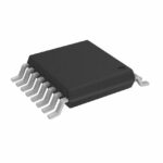 DG308BDQ-T1
The activity of extra discounts on wholesale prices is in full swing…
Please fill in your contact information and we will send you the latest wholesale price list.





