 ChipApex | Global Electronic Components Supplier
SEARCH
Search Product
Search Post
— IC芯片 | 连接器 | 传感器 | 被动器件 —
Search productSearch post
— IC芯片 | 连接器 | 传感器 | 被动器件 —
Consult the customer manager about the wholesale price.
consultation hotline:86-132-6715-2157
email:[email protected]
Contact the product manager for consultation. One-stop consultation is available.
Do you want a lower wholesale price? Please send us your inquiry and we will reply immediately.
The DG309BDQ-T1 is a quad single-pole single-throw (SPST) analog switch from the DG308B/DG309B series, manufactured by Vishay Siliconix. It features a TSSOP-16 surface-mount package and operates within an extended temperature range of -40 °C to +85 °C. The device supports dual supply voltages up to ±22 V or single supplies up to 44 V. Key electrical parameters include a maximum on-resistance of 85 Ω at room temperature under ±15 V supplies, with a turn-on time of 200 ns and turn-off time of 150 ns. Power dissipation in the TSSOP package is rated at 640 mW.
Verify component authenticity through authorized distributors or direct manufacturer channels. Confirm RoHS compliance status as standard suffixes may vary. Check datasheet revision history for potential parameter updates. Validate package marking against official documentation to ensure correct identification before procurement.
Select this part when a normally closed SPST configuration is required. Ensure supply voltage does not exceed ±22 V for continuous operation. Verify thermal management capabilities given the 640 mW power dissipation limit in the TSSOP-16 package. Consider the 85 Ω on-resistance maximum for signal integrity requirements.
This component belongs to the DG308B/DG309B family of improved quad CMOS analog switches. It serves as the normally closed variant, contrasting with the DG308B which is normally open. Both devices share identical pinouts and electrical characteristics except for their default logic states.
DG309BDQ-E3: Lead-free version of the same component.
The DG309BDQ-T1 consists of four normally closed switches that open when the logic input is high.
Yes, it supports single supply operation ranging from 4 V to 44 V, though on-resistance values differ from dual-supply specifications.
The analog signal range extends from the negative supply rail to the positive supply rail, supporting up to ±22 V.
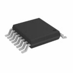 DG309BDQ-T1
The activity of extra discounts on wholesale prices is in full swing…
Please fill in your contact information and we will send you the latest wholesale price list.





