 ChipApex | Global Electronic Components Supplier
SEARCH
Search Product
Search Post
— IC芯片 | 连接器 | 传感器 | 被动器件 —
Search productSearch post
— IC芯片 | 连接器 | 传感器 | 被动器件 —
Consult the customer manager about the wholesale price.
consultation hotline:86-132-6715-2157
email:[email protected]
Contact the product manager for consultation. One-stop consultation is available.
Do you want a lower wholesale price? Please send us your inquiry and we will reply immediately.
The DG309BDQ is a quad single-pole single-throw (SPST) analog switch manufactured by Vishay Siliconix in a 16-pin TSSOP package. It operates with dual supplies up to ±22 V or single supplies up to 44 V, supporting analog signals within the supply range. The device features a maximum on-resistance of 85 Ω at room temperature and 100 Ω across the full -40 °C to +85 °C operating range. Switching times are rated at a maximum of 200 ns for turn-on and 150 ns for turn-off. Supply current is limited to 5 µA maximum, and it includes charge injection compensation.
Verify the specific suffix 'DQ' confirms the 16-lead Thin Shrink Small Outline Package (TSSOP). Confirm RoHS compliance status if required, as non-compliant versions exist without the '-E3' designation. Ensure the ordering code matches the normally closed function of the DG309B series rather than the normally open DG308B.
Select this component for applications requiring a normally closed analog path controlled by standard CMOS logic levels. Verify that the maximum on-resistance of 85 Ω meets signal integrity requirements. Ensure the operating voltage does not exceed the ±22 V absolute maximum rating to prevent permanent damage.
This part belongs to the DG308B/DG309B family of improved quad CMOS analog switches. It serves as the normally closed counterpart to the DG308BDQ. Both devices share identical electrical characteristics and pinouts but differ in their default logic states.
DG309BDJ-E3
The DG309BDQ is a normally closed switch; the channels conduct when the logic input is low (≤ 3.5 V) and block when the input is high (≥ 11 V).
Yes, the device supports single-supply operation with a maximum voltage of 44 V, though on-resistance values increase compared to dual-supply configurations.
The maximum power dissipation for the 16-pin Narrow SOIC and TSSOP packages is 640 mW.
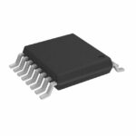 DG309BDQ
The activity of extra discounts on wholesale prices is in full swing…
Please fill in your contact information and we will send you the latest wholesale price list.





