 ChipApex | Global Electronic Components Supplier
DG612DJ-E3
Search Product
Search Post
— IC芯片 | 连接器 | 传感器 | 被动器件 —
Search productSearch post
— IC芯片 | 连接器 | 传感器 | 被动器件 —
Consult the customer manager about the wholesale price.
consultation hotline:86-132-6715-2157
email:[email protected]
Contact the product manager for consultation. One-stop consultation is available.
Do you want a lower wholesale price? Please send us your inquiry and we will reply immediately.
The DG612DJ-E3 is a high-speed, low-glitch analog switch from the Vishay Siliconix DG611 family. It features four independently controlled single-pole single-throw (SPST) channels built on a proprietary D/CMOS process combining lateral DMOS FETs with CMOS control logic. The device responds to opposite logic levels compared to the DG611. Key electrical parameters include a maximum on-resistance of 45 Ω at room temperature and 60 Ω across the full industrial range (-40 °C to 85 °C). Turn-on time is typically 12 ns with a maximum of 25 ns under standard test conditions. Charge injection is limited to ±2 pC typical. It supports dual supplies ranging from V+ = 5 V to 21 V and V- = -10 V to 0 V, or single supply operation. Quiescent power consumption is extremely low at 1.2 nW typical.
Verify the suffix 'E3' indicates lead-free and RoHS compliance when sourcing. Confirm the 'D' suffix corresponds to the 16-pin Narrow SOIC package variant. Ensure the operating environment stays within the specified -40 °C to 85 °C temperature range for guaranteed parameter limits. Check absolute maximum ratings regarding forward diode current clamping if input signals exceed supply rails.
Select this component over the DG611 when inverted control logic is required for the specific circuit design. Consider the DG613 if normally closed switches are needed alongside normally open ones. Verify that the 18 Ω typical on-resistance meets the insertion loss requirements for the target analog signal path. Ensure the 500 MHz bandwidth is sufficient for the highest frequency components of the signal being switched.
This part belongs to the DG611/DG612/DG613 family of high-speed analog switches. The DG612 specifically provides the inverse logic function of the DG611 while sharing identical physical characteristics and pinouts. The family utilizes a D/CMOS process to achieve speed and low power simultaneously, distinguishing it from standard CMOS or DMOS-only alternatives.
The DG611DJ-E3 is electrically compatible but requires logic inversion. The DG613 offers mixed NO/NC configurations. No direct cross-brand substitutes are confirmed in the provided documentation.
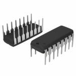 DG612DJ-E3
The activity of extra discounts on wholesale prices is in full swing…
Please fill in your contact information and we will send you the latest wholesale price list.





