 ChipApex | Global Electronic Components Supplier
SEARCH
Search Product
Search Post
— IC芯片 | 连接器 | 传感器 | 被动器件 —
Search productSearch post
— IC芯片 | 连接器 | 传感器 | 被动器件 —
Consult the customer manager about the wholesale price.
consultation hotline:86-132-6715-2157
email:[email protected]
Contact the product manager for consultation. One-stop consultation is available.
Do you want a lower wholesale price? Please send us your inquiry and we will reply immediately.
The DLP-HS-FPGA-A is a compact prototyping module featuring the Xilinx XC3S200A-4FTG256C FPGA and Micron 32M x 8 DDR2 SDRAM. It utilizes an FTDI FT2232H dual-channel USB interface for configuration and data transfer. The board provides 63 user I/O channels, including 24 differential pairs and 8 global clocks. A built-in SPI Flash loader allows direct bit file programming via USB 2.0 without external programmers. Power is supplied via USB or a 5V barrel jack, with onboard regulators generating required voltages.
Verify the specific revision level (Rev. 2.0) against project requirements. Confirm compatibility with Windows operating systems for the BitLoadApp software utility used for SPI Flash programming. Ensure availability of the free ISE WebPACK tools for design synthesis and simulation. Check for necessary USB drivers for the target host PC environment.
Select this module for applications requiring a low-cost, compact FPGA solution with integrated memory and USB connectivity. The XC3S200A offers 4,032 equivalent logic cells and 16 dedicated multipliers. Consider the 50-pin DIP interface for easy integration into breadboards or custom sockets. Verify that the 200,000 gate count meets the complexity of the intended design before finalizing selection.
This module is based on the Xilinx Spartan™ 3A family, specifically designed for rapid proof-of-concept development. It integrates Future Technology Devices International’s FT2232H IC to provide both configuration and runtime communication capabilities. The design supports migration to larger Spartan™ 3A devices like the XC3S400A on the same PCB footprint.
The datasheet notes that the XC3S400A from the Xilinx Spartan™ 3A family is pin-compatible and will work on the current PCB design. Contact DLP Design for details regarding this migration. No other direct substitute part numbers are provided in the documentation.
The FPGA can be configured by loading a bit file directly to the onboard SPI Flash via the USB interface using the BitLoadApp software. Alternatively, it can be programmed using a traditional JTAG cable connected to the JTAG header.
The module can be powered via the host PC's USB port or through an external 5-volt power supply connected to the onboard standard barrel connector. Onboard voltage regulators generate all required power supply voltages from this single source.
The maximum sink/source current on any I/O pin is 24 mA when using the LVTTL I/O standard.
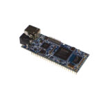 DLP-HS-FPGA-A
The activity of extra discounts on wholesale prices is in full swing…
Please fill in your contact information and we will send you the latest wholesale price list.






