 ChipApex | Global Electronic Components Supplier
SEARCH
Search Product
Search Post
— IC芯片 | 连接器 | 传感器 | 被动器件 —
Search productSearch post
— IC芯片 | 连接器 | 传感器 | 被动器件 —
Consult the customer manager about the wholesale price.
consultation hotline:86-132-6715-2157
email:[email protected]
Contact the product manager for consultation. One-stop consultation is available.
Do you want a lower wholesale price? Please send us your inquiry and we will reply immediately.
The DLP-HS-FPGA2 is a compact prototyping module featuring the Xilinx XC3S400A-4FTG256C FPGA. It integrates Micron 32M x 8 DDR2 SDRAM and an FTDI FT2232H USB interface for configuration and data transfer. The module provides 63 user I/O channels, including 24 differential pairs and 8 global clocks. Power is supplied via USB or a 5V external barrel jack. Key specifications include 8,064 equivalent logic cells, 7,168 flip-flops, 360K block RAM bits, and 20 dedicated multipliers.
Verify the specific revision of the datasheet (Rev. 1.7) to ensure compatibility with current software utilities like BitLoadApp and MPROG. Confirm that the host PC environment supports the required Windows operating systems for driver installation and bit file loading. Ensure proper static precautions are observed during handling to prevent damage to the module components.
Select the DLP-HS-FPGA2 over the standard DLP-HS-FPGA if higher logic density is required, as it utilizes the XC3S400A device offering double the logic cells and multipliers. Consider the module's small footprint (3.0 x 1.2-inch PCB) for space-constrained applications. Verify that the 63 available user I/O pins meet the interface requirements for the target design.
This module is part of the DLP Design HS-FPGA series, designed for rapid proof of concept and educational use. It serves as a bridge between host PCs and FPGA designs using the Xilinx ISE WebPACK tools. The platform simplifies development by integrating USB connectivity for both configuration and runtime communication, eliminating the need for separate programming cables.
Public confirmed substitute part numbers are not available in the provided documentation. Users requiring similar functionality should evaluate other low-cost FPGA prototyping modules from DLP Design or alternative manufacturers offering comparable Spartan 3A-based solutions with integrated USB interfaces.
The FPGA can be configured by writing the bit file directly to the onboard SPI Flash via the USB interface using the BitLoadApp software. Alternatively, traditional JTAG programming is supported via the dedicated JTAG header.
The module can be powered either through the host PC's USB port or via an external 5-volt power supply connected to the onboard barrel jack. Onboard voltage regulators generate all necessary supply voltages from this single source.
Yes, the reference design includes a DDR2 SDRAM interface block that allows read and write access to the memory via USB commands. Access requires initializing the memory first, and data transfers occur in 4-byte bursts.
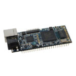 DLP-HS-FPGA2
The activity of extra discounts on wholesale prices is in full swing…
Please fill in your contact information and we will send you the latest wholesale price list.




