 ChipApex | Global Electronic Components Supplier
DM81LS97AN
Search Product
Search Post
— IC芯片 | 连接器 | 传感器 | 被动器件 —
Search productSearch post
— IC芯片 | 连接器 | 传感器 | 被动器件 —
Consult the customer manager about the wholesale price.
consultation hotline:86-132-6715-2157
email:[email protected]
Contact the product manager for consultation. One-stop consultation is available.
Do you want a lower wholesale price? Please send us your inquiry and we will reply immediately.
The DM81LS97AN is a low-power-Schottky TTL octal buffer manufactured by onsemi. It features eight two-input buffers with active LOW output enables, providing true data at the outputs. The device utilizes a 20-Lead Plastic Dual-In-Line Package (PDIP). Recommended operating conditions specify a supply voltage of 4.75V to 5.25V and an operating temperature range of 0°C to +70°C. DC electrical characteristics include a HIGH level output current of -5.2 mA and a LOW level output current of 24 mA.
Verify component authenticity through authorized distributors or official manufacturer channels. Confirm that the part number matches the specific DM81LS97AN designation. Check datasheet revisions for any updates to electrical parameters or pin configurations. Ensure compliance with RoHS directives if required for the specific application environment.
Select this component when an octal buffer with separate enable controls for four outputs each is required. Compare propagation delays against system timing requirements. Evaluate power dissipation specifications relative to thermal constraints. Consider the PDIP package dimensions for PCB layout compatibility.
This device belongs to the 81LS series of logic components. It shares functional similarities with the DM81LS95A and DM81LS96A but differs in its enable configuration. The DM81LS97A uniquely separates enable lines into two groups, unlike the common enable found in other variants within the same family.
DM81LS95AN
The DM81LS97AN has two active LOW enable inputs: G1 controls outputs Y1-Y4, and G2 controls outputs Y5-Y8.
It acts as an octal buffer, passing input data to the outputs when enabled, without inversion.
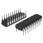 DM81LS97AN
The activity of extra discounts on wholesale prices is in full swing…
Please fill in your contact information and we will send you the latest wholesale price list.





