 ChipApex | Global Electronic Components Supplier
SEARCH
Search Product
Search Post
— IC芯片 | 连接器 | 传感器 | 被动器件 —
Search productSearch post
— IC芯片 | 连接器 | 传感器 | 被动器件 —
Consult the customer manager about the wholesale price.
consultation hotline:86-132-6715-2157
email:[email protected]
Contact the product manager for consultation. One-stop consultation is available.
Do you want a lower wholesale price? Please send us your inquiry and we will reply immediately.
The DMB53D0UV-13 is an N-channel enhancement mode MOSFET combined with an NPN transistor in a single SOT563 package. It features a drain-source voltage of 50V and continuous drain current of 160mA. The device has a maximum gate threshold voltage of 1.0V, static on-resistance up to 5Ω, and total power dissipation of 250mW. Operating temperature ranges from -55°C to +150°C.
Verify the specific ordering suffix matches the required packaging quantity. Confirm that the component meets all necessary automotive or industrial qualification standards if applicable. Ensure compatibility with the target PCB footprint and soldering profile during integration.
Select this component when space constraints require combining MOSFET and BJT functions in a single footprint. Consider the low gate threshold voltage for low-power logic interfaces. Evaluate the thermal resistance and power dissipation limits against the expected operating load conditions.
This part belongs to Diodes Incorporated's discrete semiconductor portfolio, specifically designed for compact electronic designs. It utilizes the SOT563 case outline to minimize board space while providing dual active devices. The product is manufactured in facilities adhering to quality management standards.
For automotive grade requirements with specific change control, refer to the related Q-suffix parts qualified to AEC-Q101. Verify pinout and electrical characteristics before substituting with other dual-transistor packages.
The MOSFET gate is protected against electrostatic discharge up to 2kV.
The standard version is qualified to JEDEC standards for high reliability. Automotive-specific versions are available with AEC-Q101 qualification.
The maximum collector-emitter breakdown voltage (VCEO) is 45V.
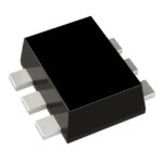 DMB53D0UV-13
The activity of extra discounts on wholesale prices is in full swing…
Please fill in your contact information and we will send you the latest wholesale price list.





