 ChipApex | Global Electronic Components Supplier

SEARCH
Search Product
Search Post
— IC芯片 | 连接器 | 传感器 | 被动器件 —
Search productSearch post
— IC芯片 | 连接器 | 传感器 | 被动器件 —
Consult the customer manager about the wholesale price.
consultation hotline:86-132-6715-2157
email:[email protected]
Contact the product manager for consultation. One-stop consultation is available.
Do you want a lower wholesale price? Please send us your inquiry and we will reply immediately.
DMN2450UFB4-7B is listed in the Single FETs, MOSFETs range at ChipApex. The manufacturer field lists Diodes Incorporated. Its product description is MOSFET N-CH 20V 1A X2-DFN1006-3. Review the specifications below when checking this part for your BOM.
The DMN2450UFB4-7B is an N-channel enhancement mode MOSFET from Diodes Incorporated, housed in a compact X2-DFN1006-3 package. It features a drain-source voltage (VDSS) of 20V and a gate-source voltage (VGSS) rating of ±12V. The device offers a maximum static drain-source on-resistance (RDS(ON)) of 0.4Ω at VGS = 4.5V with a continuous drain current (ID) of 1.0A at +25°C. Additional RDS(ON) specifications include 0.5Ω at VGS = 2.5V (0.9A ID) and 0.7Ω at VGS = 1.8V (0.8A ID). The gate threshold voltage ranges from 0.5V to 0.9V. Total gate charge is 0.6nC at VGS = 4.5V and 1.3nC at VGS = 10V. Operating temperature spans -55°C to +150°C.
Verify the specific ordering suffix against official documentation to confirm reel size and tape pitch. The -7B suffix indicates a 7-inch reel with 10,000 units per reel. Confirm RoHS compliance status and moisture sensitivity level requirements prior to procurement. Ensure the supplier provides traceability data consistent with manufacturer standards.
Select this component when low on-resistance is critical for minimizing conduction losses in small form factor designs. The low gate threshold voltage supports operation with lower logic drive levels. Evaluate thermal dissipation capabilities based on the specific PCB copper area and ambient conditions, as power handling varies with mounting configuration.
This part belongs to the DMN series of N-channel enhancement mode MOSFETs manufactured by Diodes Incorporated. It utilizes silicon technology and is designed for surface mount applications. The X2-DFN1006-3 package provides a lead-free, halogen-free, and antimony-free solution compliant with environmental directives.
Consult official substitution guides for verified alternatives. Cross-referencing requires matching VDSS, ID, RDS(ON), package type, and pinout configuration to ensure functional compatibility without redesigning the PCB layout.
The maximum pulsed drain current is 3.0A, specified with a 10μs pulse duration and a 1% duty cycle.
The on-resistance increases as the junction temperature rises. Typical curves show higher RDS(ON) values at elevated temperatures such as 125°C and 150°C compared to room temperature.
Yes, the device features an ESD protected gate structure.
Explore related parts through FETs, MOSFETs, Transistors, Discrete Semiconductor Products, all product categories.
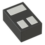 DMN2450UFB4-7B

The activity of extra discounts on wholesale prices is in full swing…
Please fill in your contact information and we will send you the latest wholesale price list.





