 ChipApex | Global Electronic Components Supplier
SEARCH
Search Product
Search Post
— IC芯片 | 连接器 | 传感器 | 被动器件 —
Search productSearch post
— IC芯片 | 连接器 | 传感器 | 被动器件 —
Consult the customer manager about the wholesale price.
consultation hotline:86-132-6715-2157
email:[email protected]
Contact the product manager for consultation. One-stop consultation is available.
Do you want a lower wholesale price? Please send us your inquiry and we will reply immediately.
The DMP31D1U-7 is a P-channel enhancement mode MOSFET manufactured by Diodes Incorporated. It features a maximum drain-source voltage (VDS) of -30 V and a gate-source voltage (VGSS) rating of ±8 V. The device supports a continuous drain current (ID) of -0.62 A at +25°C, with a pulsed drain current (IDM) capability of -2 A. Static drain-source on-resistance (RDS(ON)) ranges from 0.6 Ω to 2 Ω depending on the gate drive voltage (-4.5 V to -1.8 V). Total power dissipation (PD) is rated at 0.46 W to 0.58 W. Operating and storage temperatures span from -55°C to +150°C.
Verify the specific ordering suffix against official Diodes Incorporated documentation to confirm packing quantity and carrier type. Confirm that the component meets all applicable regulatory requirements for your target market. Ensure proper handling procedures are followed due to the ESD sensitive nature of the gate terminal. Validate thermal management strategies based on the specified junction-to-ambient thermal resistance values under your specific board layout conditions.
Select this component when a compact SOT-23 package is required for low-voltage P-channel switching applications. Evaluate the RDS(ON) specifications relative to your expected load current and available gate drive voltage levels. Consider the total gate charge and switching times if high-frequency operation is necessary. Verify that the -30 V breakdown voltage provides adequate margin for your system's supply rails.
This part belongs to the DMP31D1U series of P-channel enhancement mode MOSFETs. It utilizes silicon technology and is housed in a standard SOT-23 surface-mount package. The device is designed to offer a balance between low conduction losses and fast switching speeds suitable for modern portable electronic designs.
Consult official Diodes Incorporated substitution guides or datasheets for verified equivalent parts. Do not assume pin-compatible alternatives without verifying electrical parameters such as VDS, ID, and RDS(ON).
The typical turn-on rise time (tR) is 11 ns, measured under conditions of VDD = -10V, RL = 10Ω, VGS = -4.5V, and RG = 6Ω.
The gate threshold voltage (VGS(TH)) exhibits negative temperature dependence, decreasing as the junction temperature increases from -55°C to +150°C.
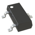 DMP31D1U-7
The activity of extra discounts on wholesale prices is in full swing…
Please fill in your contact information and we will send you the latest wholesale price list.





