ChipApex | Global Electronic Components Supplier
SEARCH
Search Product
Search Post
— IC芯片 | 连接器 | 传感器 | 被动器件 —
Search productSearch post
— IC芯片 | 连接器 | 传感器 | 被动器件 —
Consult the customer manager about the wholesale price.
consultation hotline:86-132-6715-2157
email:[email protected]
Contact the product manager for consultation. One-stop consultation is available.
Do you want a lower wholesale price? Please send us your inquiry and we will reply immediately.
The DMT10H003SPSW is a 100V N-channel enhancement mode MOSFET manufactured by Diodes Incorporated. It features a maximum drain-source voltage (BVDSS) of 100V and a gate-source voltage (VGSS) rating of ±20V. The device offers a typical static drain-source on-resistance (RDS(ON)) of 2.2mΩ at VGS=10V and ID=30A, with a maximum of 3mΩ under the same conditions. At VGS=6V and ID=25A, RDS(ON) is typically 3.4mΩ with a maximum of 5mΩ. Continuous drain current (ID) reaches 152A at TC=+25°C and 121A at TC=+70°C. Pulsed drain current (IDM) is rated at 608A. Total power dissipation (PD) is 139W at TC=+25°C. Thermal resistance from junction to case (RθJC) is 0.9°C/W.
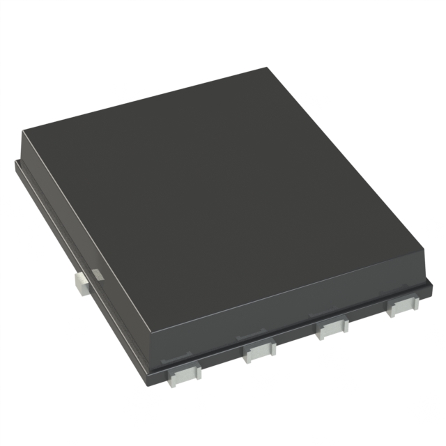
Verify the specific ordering suffix '-13' corresponds to the Tape & Reel carrier configuration containing 2,500 units per reel. Confirm that the component utilizes the PowerDI5060-8 (SWP) Type Q package variant. Ensure compliance requirements such as RoHS, Halogen-free, and Antimony-free status are validated against the manufacturer's quality definitions before procurement.
Select this component when designing circuits requiring a 100V N-channel MOSFET with low conduction losses. The device supports continuous currents up to 152A at case temperatures of +25°C. Consider the thermal resistance characteristics and the specific RDS(ON) values at VGS=10V and VGS=6V to match gate drive capabilities. Verify that the operating temperature range of -55°C to +150°C aligns with the system environment.
This part belongs to the DMT series of N-channel enhancement mode MOSFETs produced by Diodes Incorporated. It is housed in the PowerDI5060-8 surface-mount package, which provides a compact footprint suitable for dense PCB layouts. The product is designed to meet automotive quality standards, with options available for AEC-Q100 qualification and IATF 16949 manufacturing facilities upon request.
Consult the manufacturer's official documentation for verified substitute part numbers within the same family or equivalent specifications. Cross-referencing should be performed based on voltage ratings, current capacity, and package dimensions to ensure mechanical and electrical compatibility.
The maximum pulsed drain current (IDM) is rated at 608A, measured with a 10µs pulse duration and a duty cycle of 1%.
Yes, the device undergoes 100% unclamped inductive switching (UIS) testing in production to ensure reliability under inductive load conditions.
The thermal resistance from junction to case (RθJC) is specified as 0.9°C/W.
 DMT10H003SPSW-13
The activity of extra discounts on wholesale prices is in full swing…
Please fill in your contact information and we will send you the latest wholesale price list.