ChipApex | Global Electronic Components Supplier
SEARCH
Search Product
Search Post
— IC芯片 | 连接器 | 传感器 | 被动器件 —
Search productSearch post
— IC芯片 | 连接器 | 传感器 | 被动器件 —
Consult the customer manager about the wholesale price.
consultation hotline:86-132-6715-2157
email:[email protected]
Contact the product manager for consultation. One-stop consultation is available.
Do you want a lower wholesale price? Please send us your inquiry and we will reply immediately.
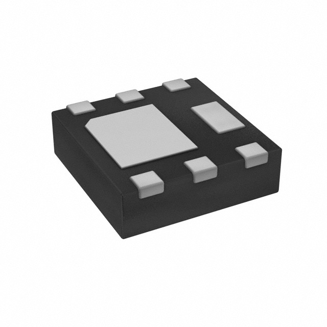
The DMT6012LFDF-13 is a 60V N-channel enhancement mode MOSFET in a U-DFN2020-6 package. It features a maximum drain-source voltage (BVDSS) of 60V and a gate-source voltage (VGSS) of ±20V. The static drain-source on-resistance (RDS(ON)) is 14mΩ max at VGS=10V and 21mΩ max at VGS=4.5V. Continuous drain current (ID) is 9.5A at TA=+25°C. Pulsed drain current (IDM) reaches 60A. Avalanche energy (EAS) is 7.9mJ with L=0.1mH. Total gate charge (Qg) is 13.6nC at VGS=10V. Operating junction temperature range is -55°C to +150°C.
Verify the specific ordering suffix '-13' corresponds to the required reel quantity of 10,000 units per reel as documented in the manufacturer's ordering information. Confirm that the U-DFN2020-6 (Type F) package dimensions and pinout match the target PCB footprint requirements. Ensure compliance with moisture sensitivity level 1 handling procedures during assembly to prevent damage during soldering processes.
Select this component when a low on-resistance N-channel MOSFET is required for 60V applications with strict height constraints. The U-DFN2020-6 package offers a small PCB footprint ideal for dense layouts. Consider the thermal resistance values and power dissipation limits relative to the expected operating ambient temperature and copper area available on the printed circuit board for adequate heat sinking.
This device belongs to Diodes Incorporated's new generation of MOSFETs designed to minimize on-state resistance while maintaining superior switching performance. It is part of the DMT series, utilizing a molded plastic green molding compound with UL flammability classification rating 94V-0. The terminals are finished with NiPdAu over a copper leadframe, ensuring solderability per MIL-STD-202 standards.
Check datasheets for alternative 60V N-channel MOSFETs in U-DFN2020-6 packages. Verify matching RDS(ON), BVDSS, and thermal characteristics before substitution. Ensure pin compatibility and package outline dimensions are identical to avoid PCB redesign.
The maximum avalanche energy (EAS) is 7.9 mJ when tested with an inductance of 0.1 mH.
For automotive applications requiring AEC-Q100/101/200 qualification or IATF 16949 manufacturing, contact Diodes Incorporated directly as standard parts may not meet these specific controls.
 DMT6012LFDF-13
The activity of extra discounts on wholesale prices is in full swing…
Please fill in your contact information and we will send you the latest wholesale price list.