 ChipApex | Global Electronic Components Supplier

SEARCH
Search Product
Search Post
— IC芯片 | 连接器 | 传感器 | 被动器件 —
Search productSearch post
— IC芯片 | 连接器 | 传感器 | 被动器件 —
Consult the customer manager about the wholesale price.
consultation hotline:86-132-6715-2157
email:[email protected]
Contact the product manager for consultation. One-stop consultation is available.
Do you want a lower wholesale price? Please send us your inquiry and we will reply immediately.
DS1306E+ is listed in the Real Time Clock range at ChipApex. The manufacturer field lists Analog Devices Inc./Maxim Integrated. Its product description is IC RTC CLK/CALENDAR SPI 20TSSOP. Review the specifications below when checking this part for your BOM.
The DS1306E+ is a serial alarm real-time clock (RTC) manufactured by Analog Devices Inc./Maxim Integrated. It provides a full binary coded decimal (BCD) clock/calendar with leap-year compensation valid up to 2100. The device includes 96 bytes of battery-backed NV RAM for data storage and two programmable time-of-day alarms. It operates on a single supply voltage ranging from 2.0V to 5.5V and supports both Motorola SPI modes 1 and 3, as well as a standard 3-wire interface. The component is housed in a 20-pin TSSOP package and functions within a commercial temperature range of 0°C to +70°C.
Verify the specific suffix 'E+' indicates a lead-free/RoHS-compliant package in the 20-pin TSSOP format. Confirm the operating temperature range is commercial (0°C to +70°C), distinct from industrial variants which carry different suffixes. Ensure the serial interface mode selection pin (SERMODE) is correctly configured for either SPI or 3-wire communication during integration.
Select the DS1306E+ when a 20-pin surface-mount package is required for space-constrained designs. Choose this model over DIP versions if PCB area is limited. Verify that the system power supply falls within the 2.0V to 5.5V range. Consider the industrial temperature variant (DS1306EN+) if operation below 0°C or above 70°C is necessary.
The DS1306 series is part of Maxim Integrated's line of serial alarm real-time clocks. The 'E' suffix denotes the 20-pin TSSOP package, while the '+' suffix signifies RoHS compliance. This component serves as a low-power timekeeping solution with integrated memory, distinguishing it from basic RTCs that lack NV RAM or dual-alarm capabilities.
Direct replacements include other DS1306 variants such as DS1306N (DIP package) or DS1306EN (Industrial temp, TSSOP). For package changes, verify pin compatibility. Cross-family alternatives may require interface adaptation due to differences in register maps or power management features.
The device switches to battery backup (VBAT) when VCC1 falls below VBAT + 0.2V. In dual-supply configurations with a rechargeable source on VCC2, it powers from the higher voltage source without write-protecting itself automatically.
VCCIF provides the logic-high level for the SDO and 32kHz output pins, allowing the DS1306 to interface easily with 3V logic systems even when powered by higher voltages.
Yes, Configuration 2 in the datasheet illustrates using a rechargeable energy source like a supercapacitor connected to VCC2, supported by a programmable trickle charger circuit.
Explore related parts through Clock/Timing, Integrated Circuits (ICs), all product categories, ChipApex homepage.
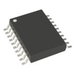 DS1306E+

The activity of extra discounts on wholesale prices is in full swing…
Please fill in your contact information and we will send you the latest wholesale price list.





