 ChipApex | Global Electronic Components Supplier
SEARCH
Search Product
Search Post
— IC芯片 | 连接器 | 传感器 | 被动器件 —
Search productSearch post
— IC芯片 | 连接器 | 传感器 | 被动器件 —
Consult the customer manager about the wholesale price.
consultation hotline:86-132-6715-2157
email:[email protected]
Contact the product manager for consultation. One-stop consultation is available.
Do you want a lower wholesale price? Please send us your inquiry and we will reply immediately.
The DS15MB200TSQ is a dual multiplexer/buffer integrated circuit designed for low-voltage differential signaling (LVDS) interfaces. Manufactured by Texas Instruments, it supports data rates up to 1.5 Gb/s with an operating supply voltage range of 3 V to 3.6 V and a typical operating current of 275 mA at 3.3 V. The device features three drivers and three receivers, accepting CML, LVDS, or LVPECL input types while providing LVDS outputs. It operates within a temperature range of -40°C to +85°C and is housed in a 48-pin WQFN package.
Verify the manufacturer designation carefully, as the component was originally developed by National Semiconductor before its acquisition by Texas Instruments. Confirm that the suffix 'TSQ' corresponds to the required automotive qualification and packaging specifications. Ensure compatibility with the 48-pin WQFN footprint during procurement planning.
Select this component when designing LVDS interfaces requiring dual multiplexing capabilities at speeds up to 1.5 Gb/s. It is suitable for systems needing jitter reduction and signal integrity improvement from sources like FPGAs. Verify that the 3.3 V nominal supply voltage aligns with the system power architecture and that the WQFN-48 package fits the board layout constraints.
This part belongs to the SCAN15MB200 family of dual multiplexer buffers. It shares functional similarities with the DS1SMB200 and DS08MB200 models, which offer comparable jitter performance but differ in maximum data rate support. The DS15MB200 specifically targets the 1.5 Gb/s segment of the LVDS interface market.
The DS15MB200TSQ/NOPB is a direct replacement variant. Other compatible devices within the same family include the SCAN15MB200TSQ/NOPB.
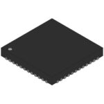 DS15MB200TSQ
The activity of extra discounts on wholesale prices is in full swing…
Please fill in your contact information and we will send you the latest wholesale price list.





