 ChipApex | Global Electronic Components Supplier

SEARCH
Search Product
Search Post
— IC芯片 | 连接器 | 传感器 | 被动器件 —
Search productSearch post
— IC芯片 | 连接器 | 传感器 | 被动器件 —
Consult the customer manager about the wholesale price.
consultation hotline:86-132-6715-2157
email:[email protected]
Contact the product manager for consultation. One-stop consultation is available.
Do you want a lower wholesale price? Please send us your inquiry and we will reply immediately.
DS26504LN+T&R is listed in the Telecom range at ChipApex. The manufacturer field lists Analog Devices Inc./Maxim Integrated. Its product description is IC TELECOM INTERFACE 64LQFP. Review the specifications below when checking this part for your BOM.
The DS26504LN+T&R is a building-integrated timing-supply (BITS) clock-recovery element and basic T1/E1 transceiver manufactured by Analog Devices Inc./Maxim Integrated. It operates within an industrial temperature range of -40°C to +85°C and is housed in a 64-pin, 10mm x 10mm LQFP package. The device accepts reference clocks of 8kHz or 19.44MHz, alongside standard T1, E1, and 64kHz composite clock inputs. It supports master clock frequencies of 16.384MHz, 12.8MHz, 8.192MHz, 4.096MHz, 2.048MHz, or 1.544MHz. The component provides 3.3V supply operation with 5V tolerant I/O and includes IEEE 1149.1 JTAG boundary scan capabilities.
Verify the specific suffix 'T&R' against official documentation to confirm tape-and-reel packaging requirements. Confirm that the LN variant meets the required -40°C to +85°C operating temperature range for your deployment environment. Ensure compatibility with existing 3.3V power rails and 5V tolerant logic levels before finalizing procurement.
Select this component when a combined BITS clock recovery and T1/E1 transceiver function is required. Verify support for specific synchronization standards such as GR378 and G.703 compliance. Consider the availability of driver source code from the manufacturer if custom firmware integration is planned. Evaluate the need for JTAG boundary scan testing during the design phase.
This part belongs to the DS26504 family of telecommunications interface ICs. It shares pin and software compatibility with the DS26502 and DS26503 models. The device serves as a foundational element for network synchronization infrastructure, bridging various clock rates and providing essential framing and transmission capabilities for digital carrier networks.
The DS26502 and DS26503 are confirmed pin and software compatible replacements within the same product family. Verify that any substitute maintains the required industrial temperature rating (-40°C to +85°C) and 64-pin LQFP package dimensions to ensure mechanical fit without PCB redesign.
The device accepts 8kHz and 19.44MHz reference clocks, in addition to T1, E1, and 64kHz composite clock inputs.
Yes, the device supports interface to CMI-coded T1/J1 and E1 signals.
Internal termination is software-selectable for 75Ω, 100Ω, 110Ω, 120Ω, and 133Ω lines on both the transmit and receive sides.
Explore related parts through Interface, Integrated Circuits (ICs), all product categories, ChipApex homepage.
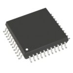 DS26504LN+T&R

The activity of extra discounts on wholesale prices is in full swing…
Please fill in your contact information and we will send you the latest wholesale price list.






