 ChipApex | Global Electronic Components Supplier
SEARCH
Search Product
Search Post
— IC芯片 | 连接器 | 传感器 | 被动器件 —
Search productSearch post
— IC芯片 | 连接器 | 传感器 | 被动器件 —
Consult the customer manager about the wholesale price.
consultation hotline:86-132-6715-2157
email:[email protected]
Contact the product manager for consultation. One-stop consultation is available.
Do you want a lower wholesale price? Please send us your inquiry and we will reply immediately.
The DS31400GN2 is a dual digital phase-locked loop (DPLL) timing integrated circuit designed for frequency conversion and synthesis. It features eight input clocks and fourteen output clocks, supporting frequencies from 2kHz to 750MHz. The device includes two independent DPLLs, seven digital frequency synthesizers, and three high-speed low-jitter analog PLLs (APLLs). Operating on a single 1.8V supply with 3.3V I/O, it provides sub-picosecond RMS output jitter via the APLLs. Packaged in a 256-pin CSBGA (17mm x 17mm), it supports CMOS, TTL, CML, LVDS, and LVPECL interfaces.
Verify the component designation against official manufacturer documentation to confirm pinout compatibility and electrical specifications. Ensure that the ordering suffix corresponds to the required lead-free and RoHS compliance status as defined in the manufacturer's current product change notifications. Cross-reference the package dimensions with the PCB footprint library prior to procurement.
Select this component when designing systems requiring dual independent clock paths with high-resolution holdover capabilities. The device is suitable for applications demanding simultaneous generation of multiple unrelated frequencies with sub-picosecond jitter. Verify that the system requires support for specific telecom standards such as G.812, G.813, or G.8262 to utilize its built-in compliance features effectively.
The DS31400 belongs to a family of high-performance timing ICs intended for telecommunications infrastructure. It serves as a central timing function or line card timing solution. The GN2 suffix indicates a specific package variant within the broader DS31400 series, housed in a 256-pin CSBGA format suitable for surface mount assembly.
Consult the manufacturer's official substitution guide for verified alternative part numbers. Ensure any replacement maintains compatibility with the 256-CSBGA package and supports the required 1.8V core voltage with 3.3V tolerant I/O levels.
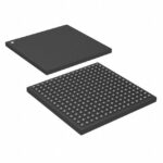 DS31400GN2
The activity of extra discounts on wholesale prices is in full swing…
Please fill in your contact information and we will send you the latest wholesale price list.





