 ChipApex | Global Electronic Components Supplier
SEARCH
Search Product
Search Post
— IC芯片 | 连接器 | 传感器 | 被动器件 —
Search productSearch post
— IC芯片 | 连接器 | 传感器 | 被动器件 —
Consult the customer manager about the wholesale price.
consultation hotline:86-132-6715-2157
email:[email protected]
Contact the product manager for consultation. One-stop consultation is available.
Do you want a lower wholesale price? Please send us your inquiry and we will reply immediately.
The DS31408GN2 is a dual DPLL timing IC designed for frequency conversion and synthesis in telecom applications. It features eight inputs and fourteen outputs, supporting frequencies from 2kHz to 750MHz with differential or CMOS/TTL formats. The device includes two independent DPLLs, seven digital frequency synthesizers, and three low-jitter APLLs generating less than 1ps RMS jitter. It integrates an IEEE 1588 clock for time synchronization. Operating at 1.8V with 3.3V I/O, it is housed in a 256-pin CSBGA package (17x17mm) and functions within a -40°C to +85°C temperature range.
Verify the specific suffix 'N2' against official Microchip documentation, as standard datasheets list 'DS31408GN'. Confirm RoHS compliance status and lead-free designation. Check for any errata associated with the manufacturing revision. Ensure the 256-CSBGA package dimensions match the design requirements.
Select this component for designs requiring dual independent clock paths with high-resolution holdover and hitless reference switching. The integrated IEEE 1588 support makes it suitable for precise time synchronization networks. Verify that the required output frequencies fall within the 2kHz to 750MHz range and that the 1.8V supply voltage aligns with the system power architecture.
The DS31408 belongs to a family of flexible timing ICs used in telecommunications infrastructure. It serves as a central timing function or line card timing solution for Stratum 2/3E/3/4E/4 standards. The device replaces multiple discrete timing components by integrating DPLLs, DFS blocks, and APLLs into a single chip.
Public confirmed substitute part numbers are not available in the provided source material.
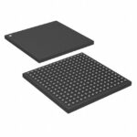 DS31408GN2
The activity of extra discounts on wholesale prices is in full swing…
Please fill in your contact information and we will send you the latest wholesale price list.






