 ChipApex | Global Electronic Components Supplier
SEARCH
Search Product
Search Post
— IC芯片 | 连接器 | 传感器 | 被动器件 —
Search productSearch post
— IC芯片 | 连接器 | 传感器 | 被动器件 —
Consult the customer manager about the wholesale price.
consultation hotline:86-132-6715-2157
email:[email protected]
Contact the product manager for consultation. One-stop consultation is available.
Do you want a lower wholesale price? Please send us your inquiry and we will reply immediately.
The DS90UB633ARTVRQ1 is an automotive-grade FPD-Link III serializer designed for high-speed video transmission. It supports 10-bit and 12-bit pixel data with input clock frequencies ranging from 56.25 MHz to 100 MHz. The device operates on a single 1.8-V supply voltage (1.71 V to 1.89 V) and features LVCMOS parallel inputs compatible with 1.8-V, 2.8-V, or 3.3-V logic levels. It includes four dedicated GPIOs and a bidirectional control channel supporting I2C communication at up to 400 kHz. Packaged in a 32-pin WQFN (5.00 mm × 5.00 mm), it is qualified under AEC-Q100 Grade 2 for ambient operating temperatures between –40°C and +105°C.
Verify the specific ordering suffix against the manufacturer's official orderable addendum to ensure correct package type and temperature grade. Confirm that the component meets AEC-Q100 Grade 2 requirements for the intended automotive application environment. Cross-reference the datasheet revision history to ensure compatibility with current design specifications.
Select this serializer when interfacing image sensors requiring up to 12-bit depth plus synchronization signals. Ensure the system utilizes a compatible deserializer from the DS90UB63x-Q1 or DS90UB66x-Q1 families. Verify that the cable length does not exceed the 15-meter drive capability and that the power supply noise remains within specified limits for stable operation.
This component belongs to the DS90UB633A-Q1 family of FPD-Link III serializers manufactured by Texas Instruments. It is specifically engineered for point-to-point connections between imagers and electronic control units. The device simplifies system architecture by transmitting video data and control information over a single differential pair.
Compatible deserializers include the DS90UB635-Q1 and DS90UB662-Q1. Ensure any replacement maintains FPD-Link III protocol compatibility and matches the required pin configuration and thermal characteristics for the existing PCB layout.
The device supports 10-bit and 12-bit payload configurations, accommodating different camera sensor resolutions and frame rates.
The IDX pin is used to assign the I2C device address via a resistor network connected to ground and the 1.8-V rail.
Yes, the MODE pin allows selection between PCLK-driven mode and external oscillator mode, where GPO3/CLKIN serves as the clock input.
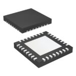 DS90UB633ARTVRQ1
The activity of extra discounts on wholesale prices is in full swing…
Please fill in your contact information and we will send you the latest wholesale price list.






