 ChipApex | Global Electronic Components Supplier
SEARCH
Search Product
Search Post
— IC芯片 | 连接器 | 传感器 | 被动器件 —
Search productSearch post
— IC芯片 | 连接器 | 传感器 | 被动器件 —
Consult the customer manager about the wholesale price.
consultation hotline:86-132-6715-2157
email:[email protected]
Contact the product manager for consultation. One-stop consultation is available.
Do you want a lower wholesale price? Please send us your inquiry and we will reply immediately.
The Altera EP1K100EFI484-2 is a Field Programmable Gate Array belonging to the ACEX 1K family. It features 4,992 logic elements and 12 Embedded Array Blocks (EABs) providing 49,152 total RAM bits. The device supports up to 333 user I/O pins and operates on a 2.5-V internal supply voltage. Packaged in a 484-pin FineLine BGA, it delivers high-density performance suitable for complex logic and memory functions.
Verify component authenticity through authorized channels as this part may be discontinued. Confirm RoHS compliance status and lead times with suppliers prior to ordering. Ensure design files are compatible with legacy development tools such as MAX+PLUS II or Quartus II for successful compilation and configuration.
Select the -2 speed grade for specific timing requirements compared to -1 or -3 grades. Ensure the 484-pin FBGA package fits the PCB footprint constraints. Verify that the 2.5-V core voltage aligns with the system power design and that MultiVolt I/O levels match connected peripherals.
This component is part of the Altera ACEX 1K series, designed for cost-efficient, high-volume applications. It combines LUT-based logic with embedded memory arrays to provide system-on-a-programmable-chip integration. The family targets applications requiring moderate logic density with flexible memory resources.
Check for pin-compatible upgrades within the ACEX 1K family, such as the EP1K50FI484-2, noting differences in I/O count and logic resources. Consider newer Intel FPGA families for long-term support, though architectural differences require full design migration.

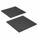 EP1K100EFI484-2
The activity of extra discounts on wholesale prices is in full swing…
Please fill in your contact information and we will send you the latest wholesale price list.



