 ChipApex | Global Electronic Components Supplier
SEARCH
Search Product
Search Post
— IC芯片 | 连接器 | 传感器 | 被动器件 —
Search productSearch post
— IC芯片 | 连接器 | 传感器 | 被动器件 —
Consult the customer manager about the wholesale price.
consultation hotline:86-132-6715-2157
email:[email protected]
Contact the product manager for consultation. One-stop consultation is available.
Do you want a lower wholesale price? Please send us your inquiry and we will reply immediately.
The Altera EP20K100TC144-3N is a Field Programmable Gate Array (FPGA) belonging to the APEX 20K family. It features a MultiCore architecture integrating look-up table (LUT) logic, product-term-based macrocells, and embedded system blocks (ESBs). The device provides 4,160 logic elements, 416 macrocells, and 53,248 maximum RAM bits. It operates at a supply voltage of 2.5 V with an I/O range of 2.5 V, 3.3 V, or 5.0 V. The component is housed in a 144-pin Thin Quad Flat Pack (TQFP) package and supports up to 92 user I/O pins.
Verify component authenticity through authorized distributors as this part may be end-of-life. Confirm RoHS compliance status and moisture sensitivity levels prior to procurement. Ensure storage conditions meet JEDDEC standards to prevent damage before reflow soldering.
Select this model for designs requiring mixed LUT and product-term logic within a 144-pin TQFP footprint. Verify that the 2.5 V internal supply voltage aligns with the target power budget. Check if the 92 available user I/O pins satisfy the interface requirements compared to other pin counts in the APEX 20K series.
This device is part of the APEX 20K family, which introduced the MultiCore architecture to Altera's programmable logic portfolio. It serves as a bridge between traditional CPLDs and high-density FPGAs, offering significant logic density and embedded memory capabilities for its time.
Publicly confirmed substitute part numbers are not available in the provided documentation. Consider modern Intel/Altera FPGA families such as Cyclone or Arria for new designs, ensuring pinout and logic resource compatibility during migration.
The EP20K100E is part of the APEX 20KE superset, offering enhanced features such as support for 1.8-V I/O, CAM, additional global clocks, and advanced clock circuitry compared to the standard EP20K100.
It integrates LUT-based logic for efficient data-path handling with product-term-based logic for complex state machines, allowing both types of functions to coexist efficiently on a single die without excessive routing overhead.
The ESB implements memory functions including dual-port RAM, FIFO buffers, ROM, and Content-Addressable Memory (CAM), providing high-speed access without reducing available logic resources.


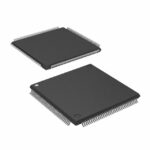 EP20K100TC144-3N
The activity of extra discounts on wholesale prices is in full swing…
Please fill in your contact information and we will send you the latest wholesale price list.



