 ChipApex | Global Electronic Components Supplier

SEARCH
Search Product
Search Post
— IC芯片 | 连接器 | 传感器 | 被动器件 —
Search productSearch post
— IC芯片 | 连接器 | 传感器 | 被动器件 —
Consult the customer manager about the wholesale price.
consultation hotline:86-132-6715-2157
email:[email protected]
Contact the product manager for consultation. One-stop consultation is available.
Do you want a lower wholesale price? Please send us your inquiry and we will reply immediately.
EPF8282ALC84-4 is listed in the Field Programmable Gate Array range at ChipApex. The manufacturer field lists Altera. Its product description is IC FPGA 68 I/O 84PLCC. Review the specifications below when checking this part for your BOM.
The EPF8282ALC84-4 is a CMOS programmable logic device from the Altera FLEX 8000 family, housed in an 84-pin PLCC package. It provides 2,500 usable gates, 282 flip-flops, 26 Logic Array Blocks (LABs), and 208 Logic Elements (LEs). The device supports up to 68 user I/O pins and operates within a voltage range of 4.75 V to 5.25 V. It features FastTrack Interconnect for predictable delays, built-in JTAG boundary-scan test circuitry compliant with IEEE Std. 1149.1-1990, and MultiVolt I/O interface capabilities. The component is designed for in-circuit reconfigurability and low standby power consumption.
This component is identified as obsolete or end-of-life by major distributors. Verification of availability requires checking secondary market suppliers or existing stock holders. Designers should confirm lead times and authenticity carefully when sourcing from non-primary channels due to the discontinued status.
Select this device for designs requiring fine-grained architecture combined with EPLD-like predictable interconnect delays. Ensure the application fits within the 208 LE capacity and 68 I/O limit. Verify that the 5V core voltage aligns with the system power supply, noting the MultiVolt capability allows flexible I/O interfacing.
The EPF8282A belongs to the FLEX 8000 family, which combines FPGA register richness with EPLD performance. This specific model represents the entry-level density in the 84-pin package options, offering 2,500 usable gates. It is part of a lineage that introduced in-circuit reconfigurability and fast continuous routing structures to the programmable logic market.
No direct public substitute part numbers are confirmed in the provided documentation. Modern replacements typically involve Intel/Altera Agilex or Cyclone families, but these require significant architectural redesign and do not offer pin-compatible alternatives.
The device contains 208 Logic Elements (LEs) arranged in 26 Logic Array Blocks (LABs).
Yes, it includes built-in Joint Test Action Group (JTAG) boundary-scan test circuitry compliant with IEEE Std. 1149.1-1990.
Yes, the MultiVolt I/O interface allows the I/O pins to be compatible with both 5.0-V and 3.3-V logic levels.
Explore related parts through Embedded, Integrated Circuits (ICs), all product categories, ChipApex homepage.


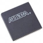 EPF8282ALC84-4

The activity of extra discounts on wholesale prices is in full swing…
Please fill in your contact information and we will send you the latest wholesale price list.



