 ChipApex | Global Electronic Components Supplier
SEARCH
Search Product
Search Post
— IC芯片 | 连接器 | 传感器 | 被动器件 —
Search productSearch post
— IC芯片 | 连接器 | 传感器 | 被动器件 —
Consult the customer manager about the wholesale price.
consultation hotline:86-132-6715-2157
email:[email protected]
Contact the product manager for consultation. One-stop consultation is available.
Do you want a lower wholesale price? Please send us your inquiry and we will reply immediately.
The onsemi FIN3385MTDX is a serializer designed to convert 28-bit parallel Low-Voltage TTL (LVTTL) data into four serial Low Voltage Differential Signaling (LVDS) streams. It operates within a supply voltage range of 3.0V to 3.6V and supports an operating temperature range from -40°C to +85°C. The device accommodates shift clock frequencies between 20MHz and 85MHz, achieving a maximum throughput of up to 2.38Gbps. It features an internal Phase-Locked Loop (PLL) requiring no external components and complies with the TIA/EIA-644 specification. The component is housed in a 56-lead Thin-Shrink Small-Outline Package (TSSOP).
Verify the specific ordering suffix against current manufacturer documentation to ensure correct packing methods and package variations. Confirm that the component meets all environmental and electrical requirements for the intended application before finalizing procurement decisions.
Select this serializer when interfacing wide parallel buses to LVDS transmission lines. Ensure the system design accounts for the required 3.3V power supply and the specific pinout configuration of the 56-lead TSSOP package. Verify compatibility with the corresponding deserializer model for complete link functionality.
This component belongs to the FIN3385/FIN3386 series, which functions as a paired serializer and deserializer solution. Originally developed by Fairchild Semiconductor, these devices are now managed under ON Semiconductor following corporate integration. The series addresses challenges associated with high-speed, wide parallel interfaces in display applications.
Check for updated part numbers due to the transition from Fairchild to ON Semiconductor naming conventions. Verify if alternative serializers within the same family meet the specific interface requirements.
The /PwrDn pin controls the power-down state. Asserting it LOW places the outputs in a high-impedance state.
The transmitter output data jitter specifications vary based on the input clock frequency, with cycle-to-cycle jitter measured at different rates such as 40MHz, 65MHz, and 85MHz.
A two-bit cycle delay is guaranteed when the Most Significant Bit (MSB) is output from the transmitter.
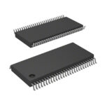 FIN3385MTDX
The activity of extra discounts on wholesale prices is in full swing…
Please fill in your contact information and we will send you the latest wholesale price list.







