ChipApex | Global Electronic Components Supplier
SEARCH
Search Product
Search Post
— IC芯片 | 连接器 | 传感器 | 被动器件 —
Search productSearch post
— IC芯片 | 连接器 | 传感器 | 被动器件 —
Consult the customer manager about the wholesale price.
consultation hotline:86-132-6715-2157
email:[email protected]
Contact the product manager for consultation. One-stop consultation is available.
Do you want a lower wholesale price? Please send us your inquiry and we will reply immediately.
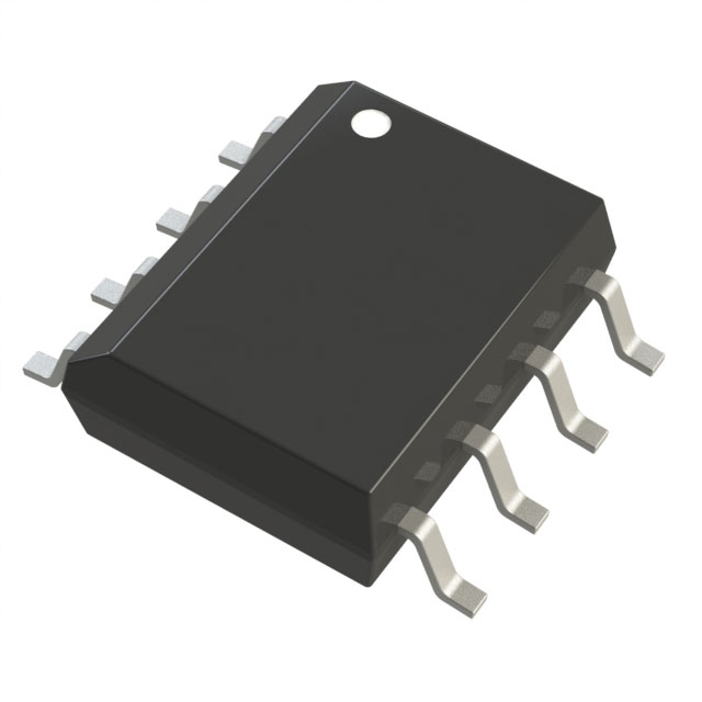
The FT24C512A-USG-B is a 512K-bit (65,536 x 8) serial EEPROM manufactured by Fremont Micro Devices Ltd. It features a standard two-wire I2C interface with Schmitt trigger inputs for noise protection. The device supports a supply voltage range of 1.8V to 5.5V and operates within an industrial temperature range of -40°C to 85°C. It offers a maximum clock frequency of 1 MHz at 2.5-5V and 400 kHz at 1.8V. Key specifications include a self-timed write cycle of 5ms maximum, high endurance of typically 1,000,000 cycles, and 100 years data retention. The USG suffix indicates an SOP-8 package in tape and reel packaging.
Verify the specific ordering code FT24C512A-USG-B against official Fremont Micro Devices documentation to confirm package type and packaging format. Ensure compatibility with system voltage levels and interface requirements before procurement. Check for any recent product change notices or lifecycle status updates directly from the manufacturer.
Select this component when a 512K-bit non-volatile memory solution is required with I2C connectivity. Consider the wide supply voltage range for flexibility in power design. Evaluate the industrial temperature rating for environmental suitability. Confirm that the SOP-8 package fits the PCB layout constraints.
This part belongs to the FT24CxxxA series of serial EEPROMs from Fremont Micro Devices. The series utilizes advanced CMOS technology for low power operation. The FT24C512A variant specifically provides 512 kilobits of storage capacity organized as 65,536 bytes. It is designed for applications requiring reliable data retention and frequent write cycles.
Compatible replacements may include other 512K-bit I2C EEPROMs from manufacturers like Microchip (e.g., AT24C512C series). Verify pinout compatibility, voltage ranges, and timing parameters before substitution. Ensure the replacement device meets the same industrial temperature and endurance specifications.
The Write Protect (WP) pin disables all programming functions when connected to VCC or VIH. Read operations remain unaffected regardless of the WP pin state.
The device includes a Power-On Reset (POR) circuit that prevents command acceptance until VCC reaches a stable value above the internal threshold. A decoupling capacitor of at least 10nF is recommended on the VCC pad.
The self-timed write cycle has a maximum duration of 5 milliseconds. During this period, the device ignores incoming commands until the write operation completes.
 FT24C512A-USG-B
The activity of extra discounts on wholesale prices is in full swing…
Please fill in your contact information and we will send you the latest wholesale price list.