 ChipApex | Global Electronic Components Supplier

SEARCH
Search Product
Search Post
— IC芯片 | 连接器 | 传感器 | 被动器件 —
Search productSearch post
— IC芯片 | 连接器 | 传感器 | 被动器件 —
Consult the customer manager about the wholesale price.
consultation hotline:86-132-6715-2157
email:[email protected]
Contact the product manager for consultation. One-stop consultation is available.
Do you want a lower wholesale price? Please send us your inquiry and we will reply immediately.
G05N06S2 is listed in the FET, MOSFET Arrays range at ChipApex. The manufacturer field lists Goford Semiconductor. Its product description is MOSFET 2N-CH 60V 5A 8SOP. Review the specifications below when checking this part for your BOM.
The G05N06S2 is a dual N-channel enhancement mode power MOSFET utilizing advanced trench technology. It features a maximum drain-source voltage of 60 V and a continuous drain current of 5 A at 25°C. The device offers low on-resistance, with a maximum value of 35 mΩ at VGS = 10V and 40 mΩ at VGS = 4.5V. Total gate charge is typically 26 nC. It operates within a junction temperature range of -55°C to 150°C and has a thermal resistance (junction-to-ambient) of 40.3°C/W.
Verify the specific package marking '05NOS' and SOP-8 dual pinout against your schematic requirements. Confirm that the 4000 pcs/tube packaging aligns with your assembly line capabilities. Ensure the component meets RoHS compliance standards required by your target market regulations before finalizing procurement.
Select this component when designing circuits requiring a compact dual MOSFET solution for 60 V systems. The low gate charge and optimized RDS(ON) make it suitable for improving efficiency in DC/DC converters. Verify that the 5 A continuous current rating and 40.3°C/W thermal resistance are sufficient for your specific thermal management design constraints.
This part belongs to Goford Semiconductor's lineup of dual N-channel enhancement mode power MOSFETs. These devices are designed to replace discrete single MOSFET pairs in space-constrained designs, offering simplified layout and matched electrical characteristics for both high-side and low-side switching roles.
No public confirmed substitute part numbers are available in the provided documentation.
The maximum pulsed drain current (IDM) is 20 A, limited by the maximum junction temperature.
Yes, the datasheet explicitly lists RoHS compliance as one of its general features.
The typical reverse recovery time (Trr) is 23 ns, measured at IF = 5A, VGS = 0V, and di/dt = 500A/us.
Explore related parts through FETs, MOSFETs, Transistors, Discrete Semiconductor Products, all product categories.
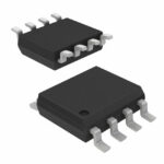 G05N06S2

The activity of extra discounts on wholesale prices is in full swing…
Please fill in your contact information and we will send you the latest wholesale price list.





