ChipApex | Global Electronic Components Supplier

SEARCH
Search Product
Search Post
— IC芯片 | 连接器 | 传感器 | 被动器件 —
Search productSearch post
— IC芯片 | 连接器 | 传感器 | 被动器件 —
Consult the customer manager about the wholesale price.
consultation hotline:86-132-6715-2157
email:[email protected]
Contact the product manager for consultation. One-stop consultation is available.
Do you want a lower wholesale price? Please send us your inquiry and we will reply immediately.
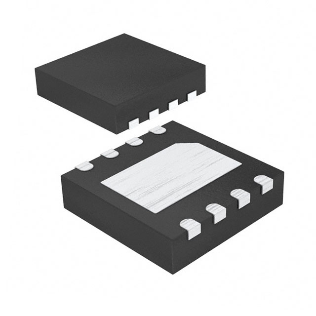
GD25B256EWIGY is listed in the Memory IC range at ChipApex. The manufacturer field lists GigaDevice Semiconductor (HK) Limited. Its product description is IC FLASH 256MBIT SPI/QUAD 8WSON. Review the specifications below when checking this part for your BOM.
The GD25B256EWIGY is a 256M-bit (32M-byte) Serial NOR Flash memory device manufactured by GigaDevice. It supports Standard, Dual, and Quad SPI interfaces with a maximum clock frequency of 133 MHz. The device operates on a single power supply voltage ranging from 2.7V to 3.6V. It features uniform sector architecture with 4K-byte sectors and 32/64K-byte blocks. Key performance metrics include a typical page program time of 0.25ms, sector erase time of 30ms, and block erase times of 0.12s or 0.15s. Data retention is specified at 20 years with a minimum endurance of 100,000 Program/Erase cycles.
Verify the specific package variant required, as the GD25B256E series includes WSON8 (6x5mm), WSON8 (8x6mm), SOP16, and TFBGA-24 options. Confirm that the ordering suffix corresponds to the desired physical footprint and lead-free status. Ensure compatibility with the host system's voltage levels, as this component requires a 2.7V to 3.6V supply range. Check for any specific automotive or industrial grade requirements if applicable to your design.
Select this component when a 256M-bit density is required with support for high-speed Quad SPI operations. It is suitable for designs needing uniform sector erasure for consistent wear leveling. Consider the WSON8 or TFBGA packages for space-constrained PCB layouts. Ensure the application does not require low-voltage operation below 2.7V, as this model is strictly within the 2.7V-3.6V range compared to other variants in the family.
The GD25B256EWIGY belongs to the GD25B256E series of Uniform Sector Dual and Quad Serial Flash memories. This series is designed to offer high performance and reliability for diverse design requirements. It shares architectural similarities with other GD25B series devices but is distinct in its 256M-bit capacity and specific voltage operating range. The 'WIGY' suffix typically denotes the WSON8 package type with specific thermal and electrical characteristics defined by GigaDevice.
GD25B256EWIGR
No, the QE bit is permanently set to 1 by default and cannot be changed. This ensures that IO2 and IO3 pins are always enabled for Quad SPI operations.
The Extended Address Register is used only when the device operates in 3-Byte Address Mode. It allows access to memory regions beyond the 128Mb limit by setting the A24 address bit.
Driving the RESET# pin low for a minimum period of 1μs will reset the flash. After the reset cycle, the device returns to standby mode, and all volatile bits return to their default power-on status.
Explore related parts through Memory, Integrated Circuits (ICs), all product categories, ChipApex homepage.
 GD25B256EWIGY

The activity of extra discounts on wholesale prices is in full swing…
Please fill in your contact information and we will send you the latest wholesale price list.