ChipApex | Global Electronic Components Supplier

SEARCH
Search Product
Search Post
— IC芯片 | 连接器 | 传感器 | 被动器件 —
Search productSearch post
— IC芯片 | 连接器 | 传感器 | 被动器件 —
Consult the customer manager about the wholesale price.
consultation hotline:86-132-6715-2157
email:[email protected]
Contact the product manager for consultation. One-stop consultation is available.
Do you want a lower wholesale price? Please send us your inquiry and we will reply immediately.
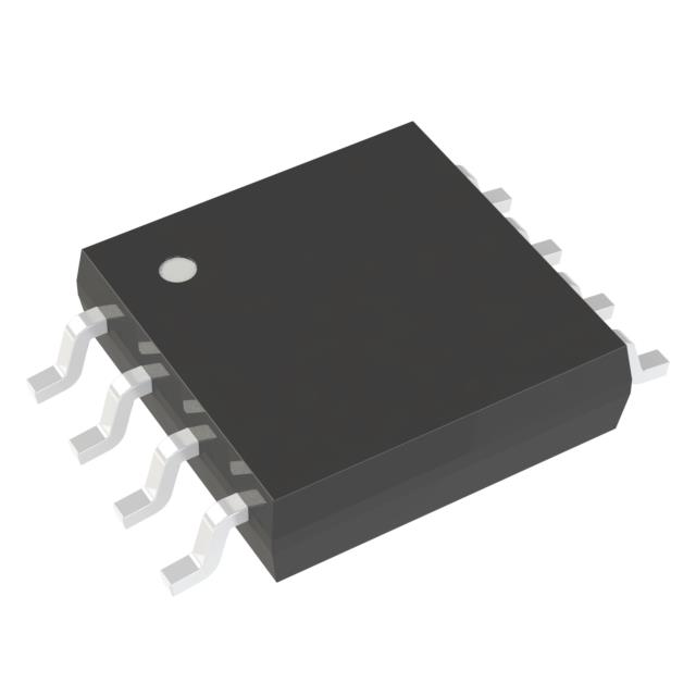
GD25LQ80CSIGR is listed in the Memory IC range at ChipApex. The manufacturer field lists GigaDevice Semiconductor (HK) Limited. Its product description is IC FLASH 8MBIT SPI/QUAD I/O 8SOP. Review the specifications below when checking this part for your BOM.
The GD25LQ80CSIGR is an 8M-bit (1M x 8) NOR flash memory manufactured by GigaDevice. It operates on a single 1.65V to 2.1V power supply and features a uniform sector architecture with 4K-byte sectors and 32/64K-byte blocks. The device supports standard, dual, and quad SPI interfaces, achieving a maximum clock frequency of 104MHz for fast read operations. It is housed in an SOP-8 package and rated for industrial temperatures ranging from -40°C to +85°C.
Verify the specific suffix 'GR' indicates tape and reel packaging when sourcing. Confirm the component status is suitable for your design lifecycle, as some variants may be marked Not Recommended for New Designs. Ensure voltage levels match the 1.65V to 2.1V requirement strictly, as this model is not compatible with 3.3V systems.
Select this part for designs requiring low-voltage operation (1.8V domain) rather than standard 3.3V NOR flashes. Consider the SOP-8 package dimensions if board space is constrained. Verify that the host controller supports the required Dual/Quad SPI commands if high-speed read performance is necessary for the application.
This component belongs to the GD25LQ80C series, which focuses on 1.8V uniform sector serial flash memories. It shares architectural similarities with other GD25Q series parts but differs in operating voltage and interface speed specifications. The GD25LQ80C is distinct from NAND flash products offered by the same manufacturer.
GD25LQ80CN2GR
In Quad SPI mode, the WP# pin functions as IO2 and the HOLD# pin functions as IO3, enabling four bidirectional data lines for faster communication.
Protection is achieved through software commands like WREN/WRDI and hardware signals like WP#. Additionally, Block Protect bits allow locking specific memory regions.
Explore related parts through Memory, Integrated Circuits (ICs), all product categories, ChipApex homepage.
 GD25LQ80CSIGR

The activity of extra discounts on wholesale prices is in full swing…
Please fill in your contact information and we will send you the latest wholesale price list.