ChipApex | Global Electronic Components Supplier

SEARCH
Search Product
Search Post
— IC芯片 | 连接器 | 传感器 | 被动器件 —
Search productSearch post
— IC芯片 | 连接器 | 传感器 | 被动器件 —
Consult the customer manager about the wholesale price.
consultation hotline:86-132-6715-2157
email:[email protected]
Contact the product manager for consultation. One-stop consultation is available.
Do you want a lower wholesale price? Please send us your inquiry and we will reply immediately.
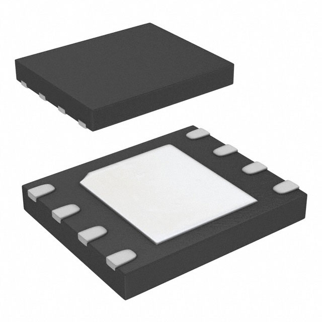
GD5F1GQ4UFYIGY is listed in the Memory IC range at ChipApex. The manufacturer field lists GigaDevice Semiconductor (HK) Limited. Its product description is IC FLASH 1GBIT SPI/QUAD 8WSON. Review the specifications below when checking this part for your BOM.
The GD5F1GQ4UFYIGY is a 1Gb (128M x 8) SPI NAND Flash memory manufactured by GigaDevice. It operates on a single power supply voltage ranging from 2.7V to 3.6V and supports standard, dual, and quad SPI interfaces with a maximum clock frequency of 120MHz. The device features a physical page size of 2048 bytes plus 128 bytes of spare area, with a typical page program time of 400µs and block erase time of 3ms. It includes an internal ECC option for error correction and is housed in an 8-WSON package measuring 6x8mm.
Verify the specific suffix 'FYIG' corresponds to the WSON-8(6x8) package and -40°C to 85°C temperature range. Confirm the datasheet revision matches the required feature set, particularly regarding the default Internal ECC state. Ensure compatibility with the host controller's SPI interface modes before procurement.
Select this component when a cost-effective alternative to parallel NAND is needed with lower pin counts than SPI NOR. It is suitable for applications requiring moderate write performance and high density. Consider the internal ECC overhead if spare area usage is critical for custom algorithms.
This part belongs to the GD5F1GQ4 series of SPI NAND Flash memories. It shares the same command set and pinout as other densities in the family, facilitating design scalability. The device utilizes a 38nm or 24nm process node depending on the specific manufacturing batch, ensuring reliability and stability for embedded applications.
GD5F1GQ4UFFIG
The Internal ECC is enabled by default upon shipment. It can be disabled by setting the ECC_EN bit to 0 via the Set Features command.
When Internal ECC is enabled, users can only program the first 64 bytes of the 128-byte spare area. The remaining 64 bytes are reserved for ECC codes but remain readable.
After power-on, the device automatically reads the first page of the first block into the cache register. This allows the host to immediately read boot code from the cache with ECC verification.
Explore related parts through Memory, Integrated Circuits (ICs), all product categories, ChipApex homepage.
 GD5F1GQ4UFYIGY

The activity of extra discounts on wholesale prices is in full swing…
Please fill in your contact information and we will send you the latest wholesale price list.