ChipApex | Global Electronic Components Supplier

SEARCH
Search Product
Search Post
— IC芯片 | 连接器 | 传感器 | 被动器件 —
Search productSearch post
— IC芯片 | 连接器 | 传感器 | 被动器件 —
Consult the customer manager about the wholesale price.
consultation hotline:86-132-6715-2157
email:[email protected]
Contact the product manager for consultation. One-stop consultation is available.
Do you want a lower wholesale price? Please send us your inquiry and we will reply immediately.
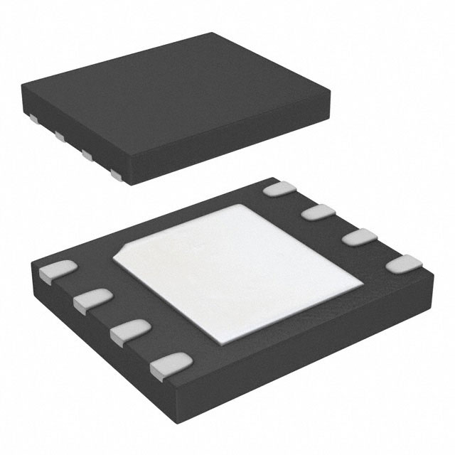
GD5F1GQ5REYIGR is listed in the Memory IC range at ChipApex. The manufacturer field lists GigaDevice Semiconductor (HK) Limited. Its product description is IC FLASH 1GBIT SPI/QUAD. Review the specifications below when checking this part for your BOM.
The GD5F1GQ5REYIGR is a 1 Gbit SPI NAND Flash memory device manufactured by GigaDevice. It features an organization of 128 M x 8 and operates with a single power supply voltage ranging from 1.7 V to 2.0 V. The component utilizes a WSON-8 package and supports standard, dual, quad, and DTR SPI interfaces with a maximum clock frequency of 104 MHz at the specified voltage. It includes internal ECC for data integrity, supports page program times of 400 us typical, and block erase times of 3 ms typical. The device operates within a temperature range of -40°C to +85°C.
Verify the specific ordering suffix to ensure compatibility with required voltage ranges and package types. Confirm that the selected variant matches the intended operating temperature range and interface requirements. Check for any recent product change notifications or end-of-life notices from the manufacturer before finalizing procurement decisions.
Select this component when a cost-effective, high-density non-volatile memory solution is needed for embedded designs. Consider the 1.8V voltage range and WSON-8 package constraints. Evaluate the need for internal ECC and specific SPI mode support (Standard, Dual, Quad, or DTR) based on system performance requirements and host controller capabilities.
This part belongs to the GD5F1GQ5xExxG series of SPI NAND Flash memories from GigaDevice. The series offers various density and voltage options, including 3.3V variants. The GD5F1GQ5REYIGR specifically targets the 1.8V application segment with industrial temperature ratings, providing a reliable storage alternative to SPI NOR and parallel NAND flash in compact form factors.
GD5F1GQ5UEYIGR
The internal ECC is enabled by default (ECC_EN=1). Users can disable it if necessary.
The HOLD# signal pauses serial communications without stopping ongoing read, program, or erase operations. It requires CS# to remain low and SCLK to be low to initiate and terminate the hold condition.
Power Lock Down Protection prevents the block lock bits from being altered even if the WP# pin is low, ensuring critical data remains protected against unintended writes during power fluctuations.
Explore related parts through Memory, Integrated Circuits (ICs), all product categories, ChipApex homepage.
 GD5F1GQ5REYIGR

The activity of extra discounts on wholesale prices is in full swing…
Please fill in your contact information and we will send you the latest wholesale price list.