ChipApex | Global Electronic Components Supplier

SEARCH
Search Product
Search Post
— IC芯片 | 连接器 | 传感器 | 被动器件 —
Search productSearch post
— IC芯片 | 连接器 | 传感器 | 被动器件 —
Consult the customer manager about the wholesale price.
consultation hotline:86-132-6715-2157
email:[email protected]
Contact the product manager for consultation. One-stop consultation is available.
Do you want a lower wholesale price? Please send us your inquiry and we will reply immediately.
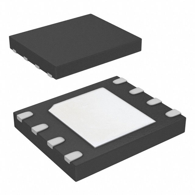
GD5F2GQ5UEYIGY is listed in the Memory IC range at ChipApex. The manufacturer field lists GigaDevice Semiconductor (HK) Limited. Its product description is IC FLASH 2GBIT SPI/QUAD. Review the specifications below when checking this part for your BOM.
The GD5F2GQ5UEYIGY is a 2 Gbit SLC NAND Flash memory device manufactured by GigaDevice. It utilizes an industry-standard SPI interface and is housed in an 8-lead WSON package. The device operates within a supply voltage range of 2.7 V to 3.6 V and supports standard, dual, quad, and DTR Quad I/O modes with a maximum clock frequency of 104 MHz at 3.3 V. It features a page size of 2048 bytes plus 128 bytes of spare area when internal ECC is disabled, or 2048 bytes plus 64 bytes when enabled. The memory array consists of 2048 blocks, each containing 64 pages.
Verify that the specific ordering suffix matches the required voltage range (2.7V–3.6V) and temperature grade (-40°C to +85°C). Confirm the package type is WSON-8 and check for any specific factory configuration requirements regarding the Quad Enable bit or OTP region before finalizing procurement.
Select this component for designs needing cost-effective high-density storage with low pin counts. Ensure the host controller supports the desired SPI mode (Standard through DTR) and has sufficient GPIO availability for the 8-pin interface. Verify power supply stability within the 2.7 V to 3.6 V range to maintain reliable operation.
This part belongs to the GD5F2GQ5xExxG series of 2 Gbit SPI NAND Flash memories. It shares the same core architecture and command set as other variants in the family, differing primarily in voltage specifications, temperature ranges, and packaging options such as TFBGA.
GD5F2GQ5UEYIHR
When internal ECC is enabled (default), the spare area is reduced to 64 bytes per page to store parity information. When disabled, the full 128-byte spare area is available for user data.
The HOLD# pin pauses serial communication without resetting the device state. It is only functional when the Quad Enable (QE) bit is cleared; otherwise, it acts as a dedicated data I/O pin (SIO3).
Explore related parts through Memory, Integrated Circuits (ICs), all product categories, ChipApex homepage.
 GD5F2GQ5UEYIGY

The activity of extra discounts on wholesale prices is in full swing…
Please fill in your contact information and we will send you the latest wholesale price list.