ChipApex | Global Electronic Components Supplier

SEARCH
Search Product
Search Post
— IC芯片 | 连接器 | 传感器 | 被动器件 —
Search productSearch post
— IC芯片 | 连接器 | 传感器 | 被动器件 —
Consult the customer manager about the wholesale price.
consultation hotline:86-132-6715-2157
email:[email protected]
Contact the product manager for consultation. One-stop consultation is available.
Do you want a lower wholesale price? Please send us your inquiry and we will reply immediately.
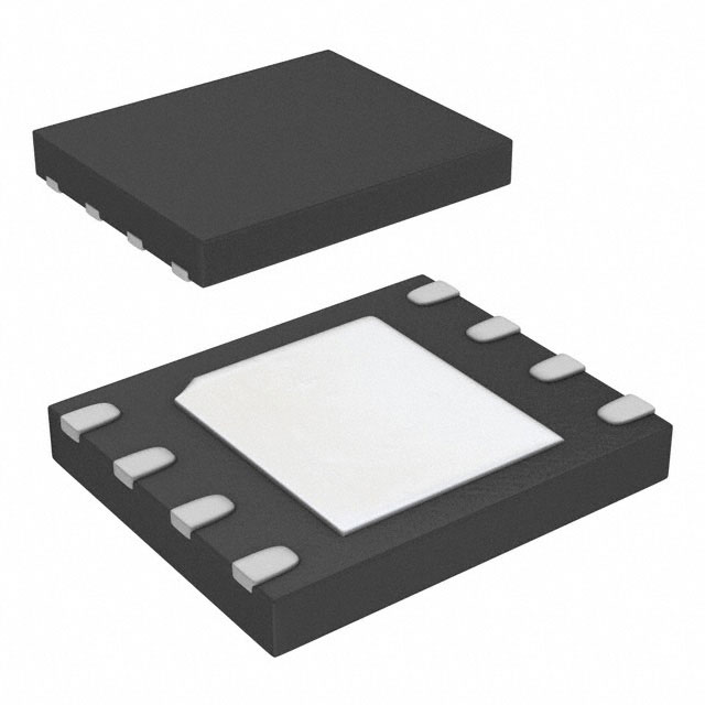
GD5F4GM8UEYIGY is listed in the Memory IC range at ChipApex. The manufacturer field lists GigaDevice Semiconductor (HK) Limited. Its product description is IC FLASH 4GBIT SPI/QUAD 8WSON. Review the specifications below when checking this part for your BOM.
The GD5F4GM8UEYIGY is a 4Gb SLC NAND Flash memory device manufactured by GigaDevice. It operates on a single power supply voltage ranging from 2.7V to 3.6V and supports Standard, Dual, Quad SPI, and DTR Quad I/O interfaces with clock frequencies up to 133MHz. The device utilizes an 8-lead WSON package (6x8mm) and functions within a temperature range of -40°C to +85°C. Key specifications include a page size of 2048 bytes plus 64 or 128 bytes spare area depending on ECC configuration, typical page program time of 320us, block erase time of 3ms, and maximum active current of 30mA.
Verify the specific ordering suffix to confirm package type and temperature grade. Ensure the system voltage aligns with the 2.7V to 3.6V requirement. Confirm interface compatibility with host controller SPI modes. Check for availability of technical documentation such as datasheets and ECAD models prior to integration.
Select this component when a cost-effective alternative to SPI-NOR or parallel NAND is required. Choose based on the need for high-speed DTR read operations or specific package constraints like the 8-WSON form factor. Consider the internal ECC feature if error correction is desired without host processing overhead.
This part belongs to the GD5F4GM8 series of SPI-NAND flash memories. It shares architectural similarities with other variants in the family but differs in voltage range and package options. The UEYIGY suffix specifically denotes the 3.3V operation and WSON8(8*6mm) packaging configuration.
GD5F4GM8UEWIGY
When internal ECC is enabled, the spare area is 64 bytes. When disabled, the spare area expands to 128 bytes.
The Data Strobe (DQS) signal indicates when output data is ready during DTR read operations. This pin is only available on the BGA24 package variant.
Explore related parts through Memory, Integrated Circuits (ICs), all product categories, ChipApex homepage.
 GD5F4GM8UEYIGY

The activity of extra discounts on wholesale prices is in full swing…
Please fill in your contact information and we will send you the latest wholesale price list.