ChipApex | Global Electronic Components Supplier

SEARCH
Search Product
Search Post
— IC芯片 | 连接器 | 传感器 | 被动器件 —
Search productSearch post
— IC芯片 | 连接器 | 传感器 | 被动器件 —
Consult the customer manager about the wholesale price.
consultation hotline:86-132-6715-2157
email:[email protected]
Contact the product manager for consultation. One-stop consultation is available.
Do you want a lower wholesale price? Please send us your inquiry and we will reply immediately.
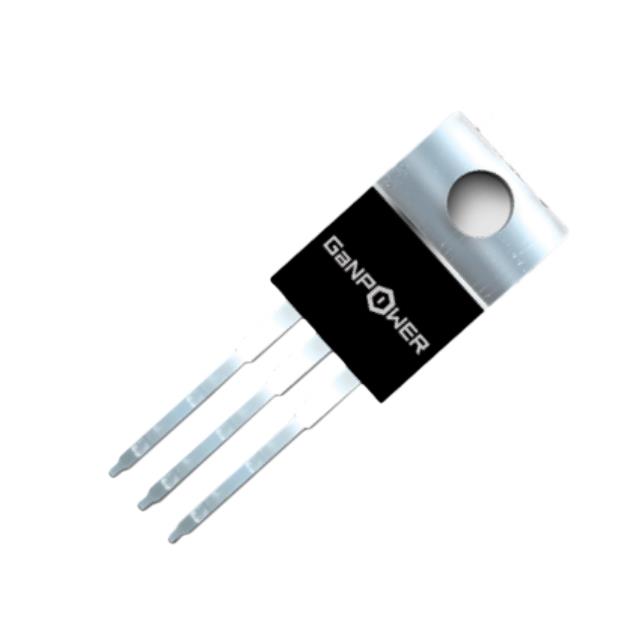
GPI65015TO is listed in the Single FETs, MOSFETs range at ChipApex. The manufacturer field lists GaNPower. Its product description is GANFET N-CH 650V 15A TO220. Review the specifications below when checking this part for your BOM.
The GPI65015TO is an N-channel enhancement-mode Gallium Nitride High Electron Mobility Transistor (GaN HEMT) manufactured by GaNPower International Inc. It features a 650V drain-source breakdown voltage and a maximum continuous drain current of 15A at a case temperature of 25°C. The device exhibits an ultra-low static on-resistance of 92mΩ and a total gate charge of 3.3nC. It operates within a junction temperature range up to 150°C and utilizes a TO-220-3 package.
Verify the specific ordering code GPI65015TO against the manufacturer's official documentation to confirm the TO-220-3 packaging configuration. Ensure that the procurement specifications align with the absolute maximum ratings, particularly the transient breakdown voltage limits and thermal resistance parameters defined in the datasheet.
Select this component for designs requiring high power density and superior efficiency at elevated switching frequencies. The zero reverse recovery charge makes it suitable for topologies where traditional silicon MOSFETs would suffer from significant tail current losses. Consider the need for specialized gate drivers capable of handling the high dv/dt characteristics inherent to GaN technology.
This device belongs to the GaNPower International Inc. portfolio of E-mode GaN on silicon transistors. Unlike conventional silicon MOSFETs, these devices utilize proprietary technology to achieve low on-state resistance without the parasitic PN junction diodes found in silicon counterparts. This structural difference fundamentally alters the switching behavior and thermal management requirements compared to legacy semiconductor technologies.
Pin-for-pin replacement with silicon MOSFETs or IGBTs is not recommended due to differences in gate driving voltage requirements and extremely high dv/dt slew rates. Specialized drivers and optimized PCB layouts are necessary to manage circuit parasitics effectively when substituting into existing designs.
Explore related parts through FETs, MOSFETs, Transistors, Discrete Semiconductor Products, all product categories.
 GPI65015TO

The activity of extra discounts on wholesale prices is in full swing…
Please fill in your contact information and we will send you the latest wholesale price list.