 ChipApex | Global Electronic Components Supplier

SEARCH
Search Product
Search Post
— IC芯片 | 连接器 | 传感器 | 被动器件 —
Search productSearch post
— IC芯片 | 连接器 | 传感器 | 被动器件 —
Consult the customer manager about the wholesale price.
consultation hotline:86-132-6715-2157
email:[email protected]
Contact the product manager for consultation. One-stop consultation is available.
Do you want a lower wholesale price? Please send us your inquiry and we will reply immediately.
GS8321Z36AGD-333I is listed in the Memory IC range at ChipApex. The manufacturer field lists GSI Technology Inc.. Its product description is IC SRAM 36MBIT PARALLEL 165FPBGA. Review the specifications below when checking this part for your BOM.
The GS8321Z36AGD-333I is a 36 Mbit Synchronous Static RAM with a 1M x 36 organization. It operates at a maximum clock frequency of 333 MHz, providing access times as fast as 4.5 ns in Flow Through mode and 2.5 ns in Pipeline mode. The device supports 2.5 V or 3.3 V core and I/O power supplies within +10%/-10% tolerance. It utilizes a JEDEC-standard 165-bump BGA package.
Verify that the specific part number suffix matches the required temperature range and voltage configuration. Confirm the package type corresponds to the design footprint. Ensure compliance with RoHS standards if applicable. Check for moisture sensitivity levels prior to soldering. Validate supply voltage compatibility with the target system architecture.
Select this component when high bandwidth and low latency are critical. Choose Pipeline mode for consistent throughput or Flow Through mode for reduced latency. Ensure the system supports the required 2.5 V or 3.3 V power rails. Verify that the PCB layout accommodates the 165-bump BGA package dimensions and pitch.
This device belongs to the GS8321Z series of NBT SRAMs from GSI Technology. It is designed for applications requiring high data rates and efficient bus utilization. The series offers various speed grades and configurations to meet diverse performance needs in embedded memory solutions.
The datasheet states the device is fully pin-compatible with pipelined and flow through NtRAM, NoBL, and ZBT SRAMs. Verify electrical characteristics and timing parameters against existing components before substitution.
NBT eliminates the need for deselect cycles when switching between read and write operations, allowing continuous data transfer without inserting dead cycles.
The Linear Burst Order (LBO) pin determines the sequence. A low state selects Linear Burst, while a high state selects Interleaved Burst.
Driving the ZZ pin high initiates Sleep mode after two clock cycles, reducing current consumption to ISB2 levels while preserving internal state.
Explore related parts through Memory, Integrated Circuits (ICs), all product categories, ChipApex homepage.
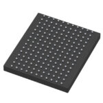 GS8321Z36AGD-333I

The activity of extra discounts on wholesale prices is in full swing…
Please fill in your contact information and we will send you the latest wholesale price list.





