 ChipApex | Global Electronic Components Supplier

SEARCH
Search Product
Search Post
— IC芯片 | 连接器 | 传感器 | 被动器件 —
Search productSearch post
— IC芯片 | 连接器 | 传感器 | 被动器件 —
Consult the customer manager about the wholesale price.
consultation hotline:86-132-6715-2157
email:[email protected]
Contact the product manager for consultation. One-stop consultation is available.
Do you want a lower wholesale price? Please send us your inquiry and we will reply immediately.
GS8342Q19BGD-357I is listed in the Memory IC range at ChipApex. The manufacturer field lists GSI Technology Inc.. Its product description is IC SRAM 36MBIT PARALLEL 165FPBGA. Review the specifications below when checking this part for your BOM.
The GS8342Q19BGD-357I is a 36Mb (37,748,736-bit) SigmaQuad-II+ SRAM manufactured by GSI Technology. It features a 2M x 18 organization with a maximum clock frequency of 357 MHz and a cycle time of 2.8 ns. The device operates on a 1.8 V core supply (VDD: 1.7 V to 1.9 V) and supports 1.5 V or 1.8 V HSTL I/O supplies (VDDQ). It utilizes a 165-bump BGA package (13 mm x 15 mm, 1 mm pitch) and includes On-Die Termination (ODT), programmable output drive strength via ZQ, and JTAG boundary scan compliance.
Verify that the specific part number suffix corresponds to the required temperature range and voltage specifications. Confirm compatibility with the host system's clocking scheme and address mapping requirements. Ensure proper termination resistor values are selected for the ZQ pin to achieve desired output impedance levels. Validate power-up sequencing protocols to maintain DLL lock stability.
Select this component for designs requiring a 2M x 18 memory configuration with high-speed synchronous operation. Consider the 165-bump BGA package constraints for PCB layout and thermal management. Evaluate the need for ODT and programmable drive strength based on trace length and signal integrity requirements. Ensure the system supports the specified HSTL I/O standards and voltage levels.
This device belongs to the SigmaQuad-II+ family of Separate I/O synchronous SRAMs. It is designed to provide economical high-performance memory solutions for networking applications. The family shares common architectural features such as pipelined reads and DDR interfaces, differing primarily in data width and speed grades.
Compatible substitutes within the same family include GS8342Q07BGD-357I, GS8342Q10BGD-357I, and GS8342Q37BGD-357I, which share identical pinouts and core functionality but differ in data bus width.
Output impedance is programmed via the ZQ pin connected to VSS through an external resistor RQ. The value of RQ must be 5 times the desired RAM output impedance, typically between 175Ω and 350Ω.
The ODT pin enables or disables On-Die Termination for Data, Byte Write, and Clock inputs. When tied High, termination is enabled; when Low or floating, it is disabled.
No, K and K cannot be set to VREF voltage or left floating. They must be driven by valid clock signals to ensure proper operation and avoid metastability.
Explore related parts through Memory, Integrated Circuits (ICs), all product categories, ChipApex homepage.
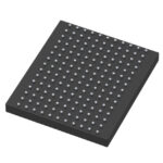 GS8342Q19BGD-357I

The activity of extra discounts on wholesale prices is in full swing…
Please fill in your contact information and we will send you the latest wholesale price list.





