ChipApex | Global Electronic Components Supplier
SEARCH
Search Product
Search Post
— IC芯片 | 连接器 | 传感器 | 被动器件 —
Search productSearch post
— IC芯片 | 连接器 | 传感器 | 被动器件 —
Consult the customer manager about the wholesale price.
consultation hotline:86-132-6715-2157
email:[email protected]
Contact the product manager for consultation. One-stop consultation is available.
Do you want a lower wholesale price? Please send us your inquiry and we will reply immediately.
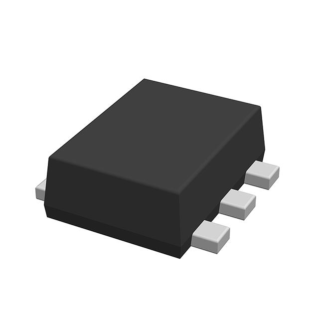
The GSBC857BDE is a dual PNP transistor manufactured by Good-Ark Semiconductor, housed in an SOT-563 surface-mount package. It features epitaxial die construction and is designed for switching and amplifier applications. Key electrical ratings include a collector-emitter voltage (VCEO) of -45 V, a collector-base voltage (VCBO) of -50 V, and a continuous collector current (IC) of -100 mA. The device has a maximum power dissipation of 150 mW and operates within a temperature range of -55°C to +150°C. DC current gain (hFE) ranges from 220 to 475 at IC=-2mA, with a transition frequency (fT) of 100 MHz.
Verify the specific ordering suffix 'BDE' corresponds to the required hFE binning level during procurement. Confirm RoHS compliance status as indicated in the manufacturer's documentation. Ensure the SOT-563 package dimensions match the target PCB footprint layout requirements before finalizing orders.
Select this component when space-constrained designs require two matched PNP transistors in a compact form factor. Consider the -45 V collector-emitter voltage rating and -100 mA current limit for circuit design. Evaluate the thermal resistance characteristics if operating near maximum power dissipation limits.
This part belongs to the GSBC857xDE series, which includes variants with different gain bins: GSBC857ADE, GSBC857BDE, and GSBC857CDE. All variants share identical electrical ratings but differ in DC current gain specifications. The BDE variant specifically targets the mid-range gain specification defined in the datasheet.
Direct replacements must match the SOT-563 package and dual PNP configuration. Verify that substitute components meet or exceed the -45 V VCEO and -100 mA IC ratings. Check pinout compatibility to ensure correct connection of the two independent transistor sections.
 GSBC857BDE
The activity of extra discounts on wholesale prices is in full swing…
Please fill in your contact information and we will send you the latest wholesale price list.