 ChipApex | Global Electronic Components Supplier

SEARCH
Search Product
Search Post
— IC芯片 | 连接器 | 传感器 | 被动器件 —
Search productSearch post
— IC芯片 | 连接器 | 传感器 | 被动器件 —
Consult the customer manager about the wholesale price.
consultation hotline:86-132-6715-2157
email:[email protected]
Contact the product manager for consultation. One-stop consultation is available.
Do you want a lower wholesale price? Please send us your inquiry and we will reply immediately.
GTL2006PW,118 is listed in the Translators, Level Shifters range at ChipApex. The manufacturer field lists NXP USA Inc.. Its product description is IC TRANSLATOR UNIDIR 28TSSOP. Review the specifications below when checking this part for your BOM.
The GTL2006PW,118 is a 13-bit translator designed to interface between 3.3 V LVTTL chip set I/O and Xeon processor GTL–/GTL/GTL+ I/O. It operates as a GTL–/GTL/GTL+ to LVTTL sampling receiver or an LVTTL to GTL–/GTL/GTL+ driver. The device supports 3.0 V to 3.6 V operation with series termination on the LVTTL outputs of 30 Ω. Propagation delay from An to Bn or Bn to An is typically 5.5 ns at CL = 50 pF and VCC = 3.3 V. The component includes ESD protection exceeding 2000 V HBM and latch-up testing exceeding 500 mA.
Verify the specific ordering code GTL2006PW against the required temperature range of –40 °C to +85 °C. Confirm that the TSSOP28 package matches your board layout constraints. Ensure that the 3.0 V to 3.6 V supply voltage requirements align with your system design. Check that LVTTL inputs are not exposed to 5 V levels as they are not 5 V tolerant.
Select this component when interfacing 3.3 V LVTTL logic with Xeon processor GTL–/GTL/GTL+ signals. It is suitable for dual processor platforms requiring health management features. Consider the 30 Ω series termination on LVTTL outputs and the non-5 V tolerant nature of the LVTTL I/O. Verify compatibility with the required operating temperature range of –40 °C to +85 °C.
The GTL2006 is part of Philips Semiconductors' (now NXP) product line of level translators. It specifically addresses the need to bridge different voltage domains in high-performance computing environments. The device replaces older translation solutions by integrating multiple channels into a single TSSOP28 package, simplifying board design for dual processor architectures.
The datasheet indicates that the GTL2006 supersedes data from December 18, 2003. No direct substitute part numbers are provided in the source material.
Yes, when the device is unpowered, the LVTTL inputs will be in a high-impedance state and will not leak to VDD if pulled high.
Yes, you can operate VTT up to 3.6 V and VREF between 0.5 V to 1.8 V at any VTT to adjust noise margins.
The enable time is deliberately slow to prevent glitches or false LOWs on the 7BOn outputs due to potentially slow rise times on open-drain I/Os like 5A and 6A.
Explore related parts through Logic, Integrated Circuits (ICs), all product categories, ChipApex homepage.
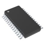 GTL2006PW,118

The activity of extra discounts on wholesale prices is in full swing…
Please fill in your contact information and we will send you the latest wholesale price list.






