 ChipApex | Global Electronic Components Supplier
GTL2034PW,112
Search Product
Search Post
— IC芯片 | 连接器 | 传感器 | 被动器件 —
Search productSearch post
— IC芯片 | 连接器 | 传感器 | 被动器件 —
Consult the customer manager about the wholesale price.
consultation hotline:86-132-6715-2157
email:[email protected]
Contact the product manager for consultation. One-stop consultation is available.
Do you want a lower wholesale price? Please send us your inquiry and we will reply immediately.
The GTL2034PW,112 is a 4-bit GTL−/GTL/GTL+ bus buffer manufactured by NXP USA Inc. It operates with a supply voltage (VCC) ranging from 3.0 V to 3.6 V and features inputs and outputs tolerant up to 3.6 V. The device supports adjustable Vref from 0.5 V to VCC/2. Propagation delays vary by protocol: for GTL−, tPLH is typically 2.8 ns and tPHL is 5.2 ns; for GTL, tPLH is 3.1 ns and tPHL is 4.1 ns; for GTL+, tPLH is 3.3 ns and tPHL is 3.6 ns. It is housed in a TSSOP14 package.
Verify the specific ordering suffix '112' against current manufacturer documentation to confirm tape-and-reel packaging details, as datasheets may list generic package types. Confirm the active status of the GTL2034PW part number with NXP or authorized distributors, as legacy products may have end-of-life implications. Ensure the application environment stays within the −40 °C to +85 °C ambient temperature range specified for reliable operation.
Select this component when interfacing between GTL−, GTL, and GTL+ domains requiring level translation and buffering. The 3.6 V I/O tolerance allows compatibility with slightly higher voltage nodes compared to standard 3.3 V parts. Consider the TSSOP14 package constraints for PCB layout if space is limited. Verify that the load capacitance requirements align with the dynamic characteristics provided for the target propagation delay performance.
The GTL2034 is part of NXP's family of Gunning Transceiver Logic (GTL) buffers. It serves as a bridge for high-speed serial and parallel interfaces utilizing GTL standards. The device simplifies system design by handling voltage level shifting internally while maintaining signal integrity across the bus. It is designed for applications where multiple GTL variants must interoperate seamlessly.
Public confirmed substitute part numbers are not available in the provided source material.
The VREF pin sets the reference voltage for the GTL inputs and outputs. It is adjustable from 0.5 V to VCC/2 to accommodate different GTL−, GTL, and GTL+ standards.
Yes, the device permits partial power-down, which can be useful for reducing power consumption in systems where only specific sections of the bus are active.
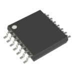 GTL2034PW,112
The activity of extra discounts on wholesale prices is in full swing…
Please fill in your contact information and we will send you the latest wholesale price list.





