 ChipApex | Global Electronic Components Supplier
GTL2034PW,118
Search Product
Search Post
— IC芯片 | 连接器 | 传感器 | 被动器件 —
Search productSearch post
— IC芯片 | 连接器 | 传感器 | 被动器件 —
Consult the customer manager about the wholesale price.
consultation hotline:86-132-6715-2157
email:[email protected]
Contact the product manager for consultation. One-stop consultation is available.
Do you want a lower wholesale price? Please send us your inquiry and we will reply immediately.
The GTL2034PW,118 is a 4-bit Gunning Transceiver Logic (GTL) to GTL bus buffer manufactured by NXP Semiconductors. It operates with a supply voltage (VCC) ranging from 3.0 V to 3.6 V and features inputs/outputs tolerant up to 3.6 V. The device supports GTL-, GTL, and GTL+ standards with an adjustable reference voltage (Vref) from 0.5 V to VCC / 2. Propagation delays are typically 3.1 ns for LOW-to-HIGH and 4.1 ns for HIGH-to-LOW transitions at VCC = 3.3 V. It includes ESD protection exceeding 2000 V HBM and latch-up protection over 500 mA.
Verify the specific ordering suffix '118' corresponds to the TSSOP14 package variant when sourcing components. Confirm that the ambient operating temperature range of -40 °C to +85 °C aligns with your system's thermal requirements. Ensure design compatibility with the required VCC supply voltage window of 3.0 V to 3.6 V. Check for any recent product status updates or obsolescence notices directly from NXP Semiconductors before finalizing procurement plans.
Select this component when interfacing between different GTL logic variants within a single voltage domain. The adjustable Vref allows optimization for specific GTL- or GTL+ noise margins. Consider the TSSOP14 package constraints regarding board space and thermal dissipation. Verify that the load capacitance requirements do not exceed the specified limits to maintain signal integrity and meet propagation delay specifications.
This device belongs to NXP's portfolio of interface buffers designed for legacy and specialized logic families. It serves as a bridge for systems transitioning between or maintaining GTL-based architectures. The component complements other level-shifting and buffering solutions offered by the manufacturer for high-speed digital interconnects.
The datasheet identifies GTL2034PWZ as a drop-in replacement for GTL2034PW. Both parts share identical electrical characteristics and pinouts but differ in packing methods, with the PWZ variant utilizing a Static Shielding Bag solution.
Yes, the device functions as a buffer for GTL-, GTL, and GTL+ standards simultaneously, allowing interoperability between these logic families.
The GTL inputs and outputs are tolerant up to 3.6 V, which exceeds the standard VCC operating range.
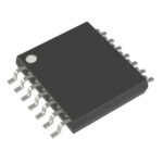 GTL2034PW,118
The activity of extra discounts on wholesale prices is in full swing…
Please fill in your contact information and we will send you the latest wholesale price list.





