ChipApex | Global Electronic Components Supplier
SEARCH
Search Product
Search Post
— IC芯片 | 连接器 | 传感器 | 被动器件 —
Search productSearch post
— IC芯片 | 连接器 | 传感器 | 被动器件 —
Consult the customer manager about the wholesale price.
consultation hotline:86-132-6715-2157
email:[email protected]
Contact the product manager for consultation. One-stop consultation is available.
Do you want a lower wholesale price? Please send us your inquiry and we will reply immediately.
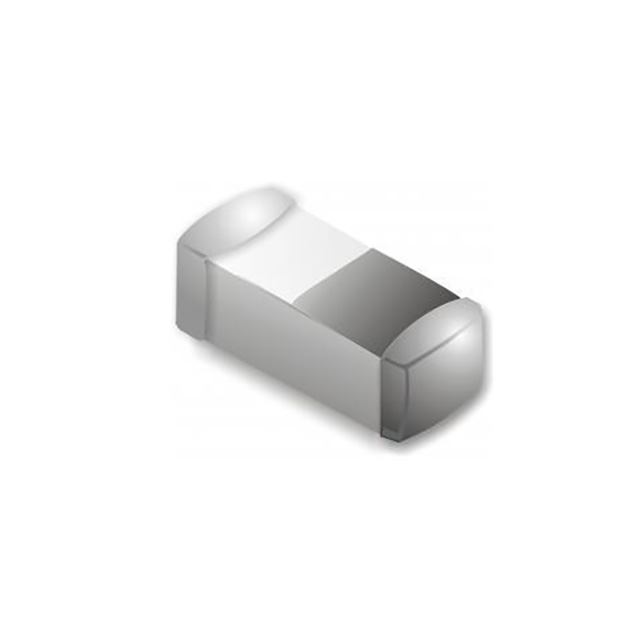
The HBLS0603-1N2S_M is an unshielded multilayer ceramic chip inductor manufactured by Max Echo Technology Corp. It features a nominal inductance of 1.2 nH with a tolerance of ±0.3 nH. The component operates within a frequency range up to 10 GHz, with self-resonant frequency specifications reaching 10 GHz. It supports a maximum DC current of 450 mA and maintains a maximum DC resistance (DCR) of 120 mOhm. The device is housed in a 0201 (0603 Metric) surface-mount package, measuring 0.6 mm in length, 0.3 mm in width, and 0.3 mm in height. It functions reliably across an operating temperature range of -55°C to +125°C.
Verify the specific manufacturer datasheet for the HBLS0603-1N2S_M to confirm electrical tolerances and thermal characteristics against application requirements. Ensure that the 0201 package dimensions align with the target PCB land pattern design. Cross-reference the maximum DC current rating of 450 mA with the actual circuit load conditions to prevent saturation or overheating during operation.
Select this component when ultra-low inductance values are required for RF applications above 100 MHz. The unshielded design minimizes parasitic effects but requires careful layout consideration to avoid coupling. The wide temperature range ensures stability in varying environmental conditions, making it suitable for consumer electronics and communication devices where space constraints are critical.
This part belongs to the HBLS series of multilayer ceramic chip inductors from Max Echo Technology Corp. The series includes various inductance values and package sizes, such as 0402 and 0603, catering to different RF power and size requirements. The HBLS0603-1N2S_M specifically targets the 0201 form factor, representing a trend toward miniaturization in high-frequency passive components.
Direct substitutes must match the 1.2 nH inductance, 0201 package, and similar DCR/Isat ratings. Verify if alternative manufacturers offer unshielded multilayer inductors with identical dimensional constraints and frequency response characteristics to ensure seamless integration without re-optimizing the RF trace layout.
 HBLS0603-1N2S_M
The activity of extra discounts on wholesale prices is in full swing…
Please fill in your contact information and we will send you the latest wholesale price list.