 ChipApex | Global Electronic Components Supplier

SEARCH
Search Product
Search Post
— IC芯片 | 连接器 | 传感器 | 被动器件 —
Search productSearch post
— IC芯片 | 连接器 | 传感器 | 被动器件 —
Consult the customer manager about the wholesale price.
consultation hotline:86-132-6715-2157
email:[email protected]
Contact the product manager for consultation. One-stop consultation is available.
Do you want a lower wholesale price? Please send us your inquiry and we will reply immediately.
HCF4042M013TR is listed in the Latches range at ChipApex. The manufacturer field lists STMicroelectronics. Its product description is IC LATCH QUAD CLOCK D 16-SOIC. Review the specifications below when checking this part for your BOM.
The HCF4042M013TR is a monolithic integrated circuit containing four clocked D latch circuits, fabricated in Metal Oxide Semiconductor technology. It features complementary buffered outputs (Q and Q) for each latch, with data transfer controlled by a common clock input and a polarity selection pin. The device operates within a supply voltage range of 3V to 20V and supports an operating temperature from -55°C to +125°C. Propagation delays vary based on voltage; at 15V, typical DATA-to-Q delay is 80ns and CLOCK-to-Q is 160ns. Input leakage current is specified at ±1µA maximum at 18V.
Verify the specific ordering suffix M013TR corresponds to the tape and reel packaging format required for automated assembly. Confirm that the component meets RoHS3 compliance standards as indicated by the manufacturer's documentation. Ensure design compatibility with the specified SOP-16 package dimensions and thermal dissipation limits during procurement planning.
Select this component when designing circuits requiring multiple latches synchronized by a shared clock signal. The availability of both Q and Q outputs simplifies differential signaling requirements. Consider the propagation delay specifications relative to the target operating voltage to ensure timing margins are met within the system architecture.
This part belongs to the HCF4042B series of quad clocked D latches manufactured by STMicroelectronics. It is available in DIP and SOP packages, with the M013TR designation specifically indicating the surface-mount SOP variant supplied in tape and reel format for high-volume manufacturing applications.
Public confirmed substitute part numbers include CD4042BM and HEF4042BT. Verify pinout compatibility and electrical parameter alignment before substitution.
When POLARITY is low, data transfers to the outputs during the low level of the clock. When POLARITY is high, data transfers during the high level of the clock.
The maximum input leakage current is specified as ±1µA at VDD = 18V and TA = 25°C.
Explore related parts through Logic, Integrated Circuits (ICs), all product categories, ChipApex homepage.
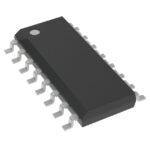 HCF4042M013TR

The activity of extra discounts on wholesale prices is in full swing…
Please fill in your contact information and we will send you the latest wholesale price list.





