 ChipApex | Global Electronic Components Supplier

SEARCH
Search Product
Search Post
— IC芯片 | 连接器 | 传感器 | 被动器件 —
Search productSearch post
— IC芯片 | 连接器 | 传感器 | 被动器件 —
Consult the customer manager about the wholesale price.
consultation hotline:86-132-6715-2157
email:[email protected]
Contact the product manager for consultation. One-stop consultation is available.
Do you want a lower wholesale price? Please send us your inquiry and we will reply immediately.
HEF4021BP-Q100U is listed in the Shift Registers range at ChipApex. The manufacturer field lists NXP USA Inc.. Its product description is IC SHIFT REGISTER 8BIT 16DIP. Review the specifications below when checking this part for your BOM.
The HEF4021BP-Q100U is an 8-bit static shift register from the Nexperia HEF4021B-Q100 family, designed for parallel-to-serial conversion. It features a synchronous serial data input (DS), clock input (CP), and asynchronous active HIGH parallel load input (PL). The device includes eight asynchronous parallel data inputs (D0 to D7) and buffered parallel outputs from the last three stages (Q5 to Q7). Each stage utilizes a D-type master-slave flip-flop with set direct (SD) and clear direct (CD) inputs. It operates within a recommended VDD power supply range of 3 V to 15 V referenced to VSS.
Verify that the specific ordering suffix matches the required package type, as the HEF4021B-Q100 family includes multiple variants such as SO16 and TSSOP16. Confirm temperature range specifications align with application requirements, noting options for -40 °C to +85 °C and -40 °C to +125 °C. Ensure compliance with JEDEC standards and ESD protection levels specified in the datasheet before finalizing procurement.
Select this component when an 8-bit shift register with automotive qualification is required. Consider the buffered parallel outputs available only on the last three stages if parallel readout is necessary. Evaluate the wide supply voltage range and Schmitt trigger clock input benefits for noisy environments or slow signal transitions. Verify package availability against board layout constraints.
This part belongs to the Nexperia HEF4021B-Q100 series of 8-bit static shift registers. The family includes various package options like SO16 and TSSOP16, all sharing the same core logic function. The Q100 designation indicates automotive grade qualification. The HEF4021BP variant specifically refers to the PDIP package version, though current documentation focuses on surface mount packages.
HEF4021BT-Q100 (SO16 package)
When the PL input is HIGH, information on D0 to D7 is asynchronously loaded into the register independent of the clock. When PL is LOW, data on the DS input is shifted into the first register position on the clock transition.
Each register stage includes a set direct (SD) and clear direct (CD) input, allowing for direct control over the state of individual flip-flops within the shift register.
Explore related parts through Logic, Integrated Circuits (ICs), all product categories, ChipApex homepage.
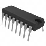 HEF4021BP-Q100U

The activity of extra discounts on wholesale prices is in full swing…
Please fill in your contact information and we will send you the latest wholesale price list.





