 ChipApex | Global Electronic Components Supplier

SEARCH
Search Product
Search Post
— IC芯片 | 连接器 | 传感器 | 被动器件 —
Search productSearch post
— IC芯片 | 连接器 | 传感器 | 被动器件 —
Consult the customer manager about the wholesale price.
consultation hotline:86-132-6715-2157
email:[email protected]
Contact the product manager for consultation. One-stop consultation is available.
Do you want a lower wholesale price? Please send us your inquiry and we will reply immediately.
The HEF4027BT,653 is a dual positive-edge triggered JK flip-flop from the Nexperia HEF4000B series. It features independent asynchronous set (nSD) and clear (nCD) inputs that override J, K, and clock signals. Data is accepted when the clock (nCP) is low and transferred on the rising edge. The device operates within a supply voltage range of 3.0 V to 15.0 V. Key electrical parameters include a propagation delay of 30 ns at 15 V, high-level output current of -3.6 mA, and low-level output current of 3.6 mA. It functions reliably between -40 °C and +85 °C.
Verify the complete ordering code including the suffix to ensure correct packaging and tape/reel specifications. Confirm that the component meets required environmental standards such as RoHS compliance. Check datasheet limits for operating temperature and voltage ranges against system requirements. Ensure ESD handling procedures are followed during assembly due to CMOS sensitivity.
Select this component for designs requiring dual JK functionality with independent preset and reset capabilities. It is suitable for applications needing robust clock signal integrity via Schmitt-trigger inputs. Consider the 3V to 15V supply range for compatibility with various logic levels. Verify pinout compatibility if replacing older CD4027 equivalents in existing layouts.
This part belongs to the Nexperia HEF4000B series, which provides CMOS logic solutions compliant with JEDEC standard JESD 13-B. The series offers standardized symmetrical output characteristics and wide supply voltage flexibility. It is designed for general-purpose digital applications requiring low power dissipation and high noise immunity in industrial environments.
Check for direct cross-reference to CD4027BE or similar dual JK flip-flops from other manufacturers. Verify pin compatibility and logical function equivalence before substitution. Ensure voltage and temperature ratings of potential replacements meet or exceed the original specifications.
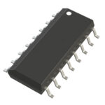 HEF4027BT,653

The activity of extra discounts on wholesale prices is in full swing…
Please fill in your contact information and we will send you the latest wholesale price list.





