 ChipApex | Global Electronic Components Supplier

SEARCH
Search Product
Search Post
— IC芯片 | 连接器 | 传感器 | 被动器件 —
Search productSearch post
— IC芯片 | 连接器 | 传感器 | 被动器件 —
Consult the customer manager about the wholesale price.
consultation hotline:86-132-6715-2157
email:[email protected]
Contact the product manager for consultation. One-stop consultation is available.
Do you want a lower wholesale price? Please send us your inquiry and we will reply immediately.
HEF4094BTT-Q100J is listed in the Shift Registers range at ChipApex. The manufacturer field lists Nexperia USA Inc.. Its product description is IC SHIFT/STORE REGISTER 16TSSOP. Review the specifications below when checking this part for your BOM.
The HEF4094BTT-Q100J is an automotive-qualified 8-stage serial shift-and-store register manufactured by Nexperia. It features a storage latch for strobing data from the serial input to parallel buffered 3-state outputs (QP0–QP7). The device operates within a recommended supply voltage range of 3.0 V to 15.0 V and supports fully static operation. Data shifts on positive-going clock transitions, with transfer to the storage register occurring when the strobe input is HIGH. Outputs assume a high-impedance OFF-state when the output enable signal is LOW. The component is housed in a TSSOP16 package (SOT403-1) and complies with AEC-Q100 Grade 1 standards.
Verify that the ordering suffix matches the required package type, as the HEF4094B-Q100 family includes both SO16 and TSSOP16 variants. Confirm that the specific application environment falls within the specified temperature ranges of -40 °C to +85 °C or -40 °C to +125 °C. Ensure design safeguards are in place, as the product is not designed for life-support or safety-critical systems without explicit written agreement.
Select this component when an 8-bit shift register with separate shift and storage clocks is required for automotive applications. The TSSOP16 package is suitable for surface-mount designs needing a thin profile. Consider the dual serial outputs (QS1 and QS2) if cascading multiple devices with varying clock rise times. Verify that the 3-state outputs meet the bus line connection requirements of the target system.
The HEF4094BTT-Q100J belongs to the HEF4094B-Q100 series of 8-stage shift-and-store registers. This series is part of Nexperia's portfolio of logic ICs qualified for automotive use under AEC-Q100 standards. The 'TT' in the model number specifically denotes the TSSOP16 plastic thin shrink small outline package (SOT403-1), distinguishing it from the SO16 variant.
HEF4094BT-Q100J
The device provides two serial outputs: QS1 outputs data on the positive-going clock edge for fast clock rise times, while QS2 outputs data on the next negative-going clock edge for slow clock rise times.
A HIGH level on the OE input allows data in the storage register to appear at the outputs. A LOW level causes the outputs to assume a high-impedance OFF-state without affecting the internal state of the registers.
Explore related parts through Logic, Integrated Circuits (ICs), all product categories, ChipApex homepage.
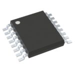 HEF4094BTT-Q100J

The activity of extra discounts on wholesale prices is in full swing…
Please fill in your contact information and we will send you the latest wholesale price list.





