 ChipApex | Global Electronic Components Supplier

SEARCH
Search Product
Search Post
— IC芯片 | 连接器 | 传感器 | 被动器件 —
Search productSearch post
— IC芯片 | 连接器 | 传感器 | 被动器件 —
Consult the customer manager about the wholesale price.
consultation hotline:86-132-6715-2157
email:[email protected]
Contact the product manager for consultation. One-stop consultation is available.
Do you want a lower wholesale price? Please send us your inquiry and we will reply immediately.
HEF4094BTTJ is listed in the Shift Registers range at ChipApex. The manufacturer field lists Nexperia USA Inc.. Its product description is IC SHIFT/STORE REGISTER. Review the specifications below when checking this part for your BOM.
The HEF4094BTTJ is an 8-bit serial-in/serial or parallel-out shift register with a storage register and 3-state outputs, manufactured by Nexperia. It operates within a supply voltage range of 3.0 V to 15.0 V and supports ambient temperatures from -40 °C to +125 °C. The device utilizes TSSOP-16 (SOT403-1) packaging. Data shifts on positive-going clock transitions, with separate clocks for the shift and storage registers. It features two serial outputs (QS1 and QS2) for cascading, accommodating both fast and slow clock rise times.
Verify the specific ordering suffix 'J' against official Nexperia documentation to confirm tape-and-reel specifications and compliance details. Ensure the selected package variant matches the required PCB footprint dimensions for SOT403-1. Confirm that the application environment remains within the specified -40 °C to +125 °C operating temperature range and does not exceed the absolute maximum ratings defined in the datasheet.
Select this component when an 8-stage shift-and-store register with 3-state outputs is required. The dual serial outputs (QS1/QS2) facilitate cascading across varying clock edge speeds. Verify compatibility with the target logic family voltage levels and ensure the TSSOP-16 package fits the design constraints. Consider the dynamic power dissipation formula for high-frequency applications.
The HEF4094BTTJ belongs to the HEF4094B series, part of the broader HEF4000 CMOS logic family. This series provides standardized symmetrical output characteristics compliant with JEDEC standard JESD 13-B. The 'TT' designation indicates the TSSOP-16 plastic thin shrink small outline package, while 'J' typically denotes reel packaging configuration.
HEF4094BT,653
Data is available at QS1 on the LOW-to-HIGH transition for fast clock edges, and at QS2 on the next HIGH-to-LOW transition for slow clock edges.
A LOW on OE causes the outputs to assume a high-impedance OFF-state. Operation of OE does not affect the state of the internal registers.
Explore related parts through Logic, Integrated Circuits (ICs), all product categories, ChipApex homepage.
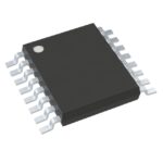 HEF4094BTTJ

The activity of extra discounts on wholesale prices is in full swing…
Please fill in your contact information and we will send you the latest wholesale price list.





