 ChipApex | Global Electronic Components Supplier

SEARCH
Search Product
Search Post
— IC芯片 | 连接器 | 传感器 | 被动器件 —
Search productSearch post
— IC芯片 | 连接器 | 传感器 | 被动器件 —
Consult the customer manager about the wholesale price.
consultation hotline:86-132-6715-2157
email:[email protected]
Contact the product manager for consultation. One-stop consultation is available.
Do you want a lower wholesale price? Please send us your inquiry and we will reply immediately.
HEF4104BT/S400118 is listed in the Translators, Level Shifters range at ChipApex. The manufacturer field lists NXP USA Inc.. Its product description is BUS DRIVER, 4-BIT. Review the specifications below when checking this part for your BOM.
The HEF4104B is a quad low-to-high voltage translator with complementary 3-state outputs. It operates within a supply voltage range of 3.0 V to 15.0 V and supports input voltages up to VDD(A) + 0.5 V. The device features inputs with clamp diodes for interfacing with voltages exceeding VDD. Propagation delays vary from 65 ns to 340 ns depending on load capacitance and supply voltage. It complies with JEDEC standard JESD 13-B and offers ESD protection exceeding 2000 V (HBM).
Verify the specific ordering suffix against the manufacturer's current catalog, as availability may vary by region. Confirm package type SOT109-1 matches design requirements. Check for any recent product status changes or obsolescence notices directly from Nexperia before finalizing procurement plans.
Select this component when designing systems that require translating signals between disparate voltage domains, specifically where inputs exceed the local supply rail. Ensure the application stays within the recommended operating conditions regarding temperature and voltage limits. Verify that the required propagation delay fits the system timing constraints under expected load capacitance.
The HEF4104B belongs to the HEF4104B family of quad translators manufactured by Nexperia. It is designed for CMOS low power dissipation applications. The device is housed in an SO16 plastic small outline package (SOT109-1). It is specified for industrial temperature ranges from -40 °C to +85 °C.
Consult official Nexperia documentation for verified substitute part numbers. Cross-reference pinouts and electrical specifications carefully when considering alternatives.
A LOW signal on the OE input causes the outputs to assume a high-impedance OFF-state.
Inputs include clamp diodes, enabling the use of current limiting resistors to interface inputs to voltages in excess of VDD(A), up to VDD(A) + 0.5 V.
Explore related parts through Logic, Integrated Circuits (ICs), all product categories, ChipApex homepage.
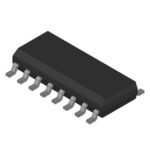 HEF4104BT/S400118

The activity of extra discounts on wholesale prices is in full swing…
Please fill in your contact information and we will send you the latest wholesale price list.






