 ChipApex | Global Electronic Components Supplier

SEARCH
Search Product
Search Post
— IC芯片 | 连接器 | 传感器 | 被动器件 —
Search productSearch post
— IC芯片 | 连接器 | 传感器 | 被动器件 —
Consult the customer manager about the wholesale price.
consultation hotline:86-132-6715-2157
email:[email protected]
Contact the product manager for consultation. One-stop consultation is available.
Do you want a lower wholesale price? Please send us your inquiry and we will reply immediately.
HI3-574AJN-5 is listed in the Analog To Digital Converters (ADC) range at ChipApex. The manufacturer field lists Renesas Electronics Corporation. Its product description is IC ADC 12BIT SAR 28DIP. Review the specifications below when checking this part for your BOM.
The HI3-574AJN-5 is a complete 12-bit Analog-to-Digital Converter (ADC) manufactured by Renesas Electronics Corporation. It utilizes a Successive Approximation Register (SAR) architecture and features an integrated +10V reference and clock oscillator. The device provides three-state outputs for direct microprocessor bus interfacing, supporting full 8-bit, 12-bit, or 16-bit data formats. It operates with analog supply voltages of ±12V to ±15V and a digital logic supply of +5V. The component is housed in a 28-lead Plastic Dual In-Line Package (PDIP) and is rated for an operating temperature range of 0°C to +75°C.
Verify that the specific ordering suffix 'JN' corresponds to the PDIP package variant as listed in the official datasheet. Confirm that the application environment remains within the specified 0°C to +75°C operating temperature range. Ensure power supplies are properly bypassed using tantalum and ceramic capacitors to maintain signal integrity and prevent noise-induced errors during conversion cycles.
Select this model when a 12-bit resolution with ±1.0 LSB linearity is sufficient for the application requirements. Consider the HI3-574AKN-5 if tighter linearity specifications of ±0.5 LSB are required. Verify that the system design accommodates the necessary bipolar or unipolar input ranges and that the microprocessor timing constraints align with the device's access and setup times.
This component belongs to the HI-X74A family of complete 12-bit A/D converters. It shares functional similarities with the HI-674A but offers a slower maximum conversion speed of 25µs compared to the 15µs capability of the HI-674A. Both variants utilize monolithic dice housed in a single package to ensure enhanced AC performance and freedom from latch-up via dielectric isolation processes.
Public documentation identifies the ISL263XX and ISL267XX families as possible substitute products. These alternatives should be evaluated based on pin compatibility and electrical parameter alignment before implementation in existing designs.
The maximum linearity error is guaranteed at ±1.0 LSB over the operating temperature range of 0°C to +75°C.
The AO input allows for byte enable or short cycle operations, providing a break-before-make action that eliminates bus contention during read operations. This mode is latched by the Start Convert input to set the conversion length.
The device supports four standard input ranges: Bipolar -5V to +5V, Bipolar -10V to +10V, Unipolar 0V to +10V, and Unipolar 0V to +20V.
Explore related parts through Data Acquisition, Integrated Circuits (ICs), all product categories, ChipApex homepage.
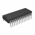 HI3-574AJN-5

The activity of extra discounts on wholesale prices is in full swing…
Please fill in your contact information and we will send you the latest wholesale price list.




