ChipApex | Global Electronic Components Supplier
SEARCH
Search Product
Search Post
— IC芯片 | 连接器 | 传感器 | 被动器件 —
Search productSearch post
— IC芯片 | 连接器 | 传感器 | 被动器件 —
Consult the customer manager about the wholesale price.
consultation hotline:86-132-6715-2157
email:[email protected]
Contact the product manager for consultation. One-stop consultation is available.
Do you want a lower wholesale price? Please send us your inquiry and we will reply immediately.
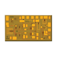
The HMC561 is a GaAs PHEMT x2 active broadband frequency multiplier chip designed for output frequencies between 8 GHz and 21 GHz. It operates on a 5 V supply (4.5 V to 5.5 V) with a typical current of 98 mA. The device dissipates up to 940 mW and functions within a temperature range of -55°C to +85°C. Packaged as a bare die in gel packaging, it features AC-coupled 50-ohm RF input and output ports. Pin 3 requires gate voltage adjustment to set the bias current.
Verify component authenticity through authorized Analog Devices channels or certified distributors. Confirm the specific die revision and gel pack integrity upon receipt. Ensure handling procedures comply with ESD standards for bare die components. Cross-reference datasheet revisions to confirm pinout and electrical specifications match design requirements before integration.
Select this component when a bare die solution is required for custom PCB layouts. Consider the HMC561LP3E if a leadless SMT package is preferred over direct die attachment. Evaluate thermal management capabilities due to the 940 mW power dissipation. Verify that the system can provide the necessary gate voltage control via Pin 3 to maintain the specified 98 mA operating current.
This part belongs to the HMC561G series of RF wireless miscellaneous components. It is manufactured using Gallium Arsenide (GaAs) technology. The device is categorized under Wireless & RF Integrated Circuits, specifically as a frequency multiplier. It serves as the die-level counterpart to packaged variants like the HMC561LP3E.
The HMC561LP3E is a documented leadless SMT package variant of the same circuit. Direct substitution requires adapting the board layout from wire bonding to surface mount soldering. Thermal and electrical characteristics remain consistent between the die and the packaged version.
 HMC561
The activity of extra discounts on wholesale prices is in full swing…
Please fill in your contact information and we will send you the latest wholesale price list.