 ChipApex | Global Electronic Components Supplier

SEARCH
Search Product
Search Post
— IC芯片 | 连接器 | 传感器 | 被动器件 —
Search productSearch post
— IC芯片 | 连接器 | 传感器 | 被动器件 —
Consult the customer manager about the wholesale price.
consultation hotline:86-132-6715-2157
email:[email protected]
Contact the product manager for consultation. One-stop consultation is available.
Do you want a lower wholesale price? Please send us your inquiry and we will reply immediately.
HMC6832ALP5LETR is listed in the Clock Buffers, Drivers range at ChipApex. The manufacturer field lists Analog Devices Inc.. Its product description is IC CLK BUFFER 2:8 3.5GHZ 28LFCSP. Review the specifications below when checking this part for your BOM.
The HMC6832ALP5LETR is a low noise, 2:8 differential fanout buffer designed for clock distribution applications. It operates within a frequency range of 10 MHz to 3500 MHz and supports supply voltages from 2.375 V to 3.6 V. The device features configurable LVPECL or pseudo-LVDS outputs, with an ultralow noise floor typically reaching −165.9 dBc/Hz at 2000 MHz. It accepts CML, LVDS, LVPECL, or CMOS inputs via AC or DC coupling. Key electrical parameters include a typical propagation delay of 201 ps (LVPECL) or 207 ps (LVDS), channel skew of ±5 ps, and a core current of 56 mA.
Verify the specific suffix 'LETR' against the manufacturer's ordering guide to confirm package type and reel specifications. Ensure compatibility with the 28-lead LFCSP (5 mm × 5 mm) footprint during procurement planning. Confirm that the selected variant matches the required thermal resistance and moisture sensitivity level (MSL3) ratings for the intended assembly process.
Select this component when low phase noise and precise timing are critical for downstream circuits like ADCs or SERDES. Choose between LVPECL and LVDS configurations based on the target system voltage requirements; LVPECL supports both 2.5 V and 3.3 V supplies, while LVDS is limited to 2.5 V. Consider the input signal format (CML/LVDS/LVPECL/CMOS) to determine necessary coupling methods and impedance matching.
The HMC6832 belongs to Analog Devices' portfolio of high-performance RF and microwave integrated circuits. As a fanout buffer, it serves as a critical link in signal chains requiring one-to-many clock distribution with minimal added jitter. It complements other clock generation and conditioning devices by providing robust buffering capabilities across a wide frequency spectrum.
Public confirmed substitute part numbers are not available in the provided documentation.
The CONFIG pin determines the output mode. Logic 0 selects LVPECL termination, while Logic 1 or an open state (internally pulled high) selects pseudo-LVDS termination.
The device has a wideband operating frequency range extending up to 3500 MHz (3.5 GHz).
Yes, the HMC6832 supports single-ended inputs with a swing range of 0.1 V to 2 V, although it is primarily designed for differential signaling.
Explore related parts through Clock/Timing, Integrated Circuits (ICs), all product categories, ChipApex homepage.
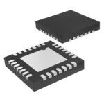 HMC6832ALP5LETR

The activity of extra discounts on wholesale prices is in full swing…
Please fill in your contact information and we will send you the latest wholesale price list.





