 ChipApex | Global Electronic Components Supplier
SEARCH
Search Product
Search Post
— IC芯片 | 连接器 | 传感器 | 被动器件 —
Search productSearch post
— IC芯片 | 连接器 | 传感器 | 被动器件 —
Consult the customer manager about the wholesale price.
consultation hotline:86-132-6715-2157
email:[email protected]
Contact the product manager for consultation. One-stop consultation is available.
Do you want a lower wholesale price? Please send us your inquiry and we will reply immediately.
The HMC856LC5 is a wideband time delay device with 5-bit digital control, designed for timing compensation and clock skew management. It supports data rates up to 28 Gbps with a maximum propagation delay of 255 ps and a resolution of 3 ps. The device operates from a single −3.3 V supply, consuming 185 mA typical current. It features differential CML inputs and outputs with internal 50 Ω termination, supporting AC or DC coupling. An output level control pin (VR) allows programmable differential output voltage swing ranging from 500 mV p-p to 1350 mV p-p. The component is housed in a 5 mm × 5 mm, 32-terminal ceramic leadless chip carrier (LCC) package.
Verify the specific ordering suffix when purchasing. The base model HMC856LC5 indicates standard packaging, while suffixes like TR denote reel packaging. Confirm moisture sensitivity level (MSL3) requirements for your assembly process. Ensure the evaluation board part number matches the component variant if testing is required before integration into the final design.
Select this component for applications requiring precise timing adjustments at data rates up to 28 Gbps. The 5-bit digital control offers sufficient granularity for most clock skew management tasks. Consider the VR pin functionality if signal amplitude adjustment is necessary within the system. Verify that the LCC package footprint fits the available PCB space constraints.
The HMC856LC5 belongs to the HMC856 series of broadband time delay devices manufactured by Analog Devices. It shares functional similarities with other members of the family but is distinguished by its specific 5-bit control interface and 28 Gbps capability. The LC5 suffix denotes the specific package type and temperature range configuration within the product line.
HMC856LC5TR and HMC856LC5TR-R5 are direct replacements differing only in packaging format (reel vs. cut tape). No other cross-model substitutes are officially documented as functionally equivalent in the provided datasheet.
The HMC856LC5 provides a delay resolution of 3 ps.
Yes, both the differential CML inputs and outputs can be AC or DC coupled.
The VR pin controls the output voltage swing between 500 mV p-p and 1350 mV p-p, which also influences rise/fall times and power consumption.


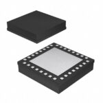 HMC856LC5
The activity of extra discounts on wholesale prices is in full swing…
Please fill in your contact information and we will send you the latest wholesale price list.



