ChipApex | Global Electronic Components Supplier
SEARCH
Search Product
Search Post
— IC芯片 | 连接器 | 传感器 | 被动器件 —
Search productSearch post
— IC芯片 | 连接器 | 传感器 | 被动器件 —
Consult the customer manager about the wholesale price.
consultation hotline:86-132-6715-2157
email:[email protected]
Contact the product manager for consultation. One-stop consultation is available.
Do you want a lower wholesale price? Please send us your inquiry and we will reply immediately.
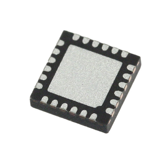
The HMC895LP4E is a monolithic microwave integrated circuit (MMIC) bandpass filter designed for surface-mount applications. It features a user-selectable passband frequency tunable between 6.8 GHz and 12.6 GHz via an analog control voltage ranging from 0 V to 14 V. The device exhibits a typical 3 dB bandwidth of approximately 10% and a 20 dB bandwidth of 22%. Key electrical specifications include a maximum insertion loss of 9 dB, a return loss of 12 dB within the 2 dB bandwidth, and an input IP3 of 28 dBm. The component operates within a temperature range of -40 °C to +85 °C and utilizes a 24-lead QFN package.
Verify component authenticity through authorized Analog Devices channels or certified distributors. Confirm that the specific lot number matches the marking on the package. Ensure handling precautions are observed due to electrostatic sensitivity. Check for RoHS compliance status as indicated in the datasheet documentation.
Select this component when a compact, single-chip tunable bandpass filter is required for frequencies between 6.8 GHz and 12.6 GHz. Consider the 9 dB insertion loss and 28 dBm input IP3 against system link budget requirements. Ensure the control voltage driver can supply the necessary current and voltage range for precise frequency and notch control.
The HMC895LP4E belongs to the Hittite Microwave Corporation product line, which was acquired by Analog Devices Inc. It serves as a direct replacement for larger, mechanically tuned filter assemblies in RF signal chains. The part is identified by the 'H895' marking on the package body.
Public confirmed substitute part numbers are not available in the provided documentation. Designers should evaluate other tunable filters from the Analog Devices portfolio if availability is a constraint.
The center frequency is controlled by applying a voltage between 0 V and 14 V to pins 9 and 10, which must be connected together externally. The low side/high side rejection notch is controlled by a separate voltage applied to pin 8.
The phase settling time to within 10 degrees is less than 200 ns, which includes a 40 ns tuning voltage ramp from the driver.
All ground leads (pins 1, 2, 4-7, 12-15, 17-19, 24) and the exposed paddle must be soldered directly to the PCB RF ground plane using sufficient via holes to connect top and bottom ground planes.
 HMC895LP4E
The activity of extra discounts on wholesale prices is in full swing…
Please fill in your contact information and we will send you the latest wholesale price list.