 ChipApex | Global Electronic Components Supplier
SEARCH
Search Product
Search Post
— IC芯片 | 连接器 | 传感器 | 被动器件 —
Search productSearch post
— IC芯片 | 连接器 | 传感器 | 被动器件 —
Consult the customer manager about the wholesale price.
consultation hotline:86-132-6715-2157
email:[email protected]
Contact the product manager for consultation. One-stop consultation is available.
Do you want a lower wholesale price? Please send us your inquiry and we will reply immediately.
The Toshiba HN1C03FU-B,LF is a dual NPN silicon epitaxial planar transistor housed in the US6 package. It features a collector-emitter voltage (VCEO) of 20 V and a collector-base voltage (VCBO) of 50 V. The device supports a maximum collector current of 300 mA with a power dissipation rating of 200 mW. Electrical characteristics include a minimum emitter-base voltage (VEBO) of 25 V and a typical reverse DC current gain (hFE) of 150 at VCE = -2 V and IC = -4 mA. The transition frequency (fT) is typically 30 MHz.
Verify the specific ordering suffix against official Toshiba Semiconductor documentation to confirm exact packaging and compliance status. Confirm that the component meets all required environmental standards for the intended deployment environment before finalizing procurement orders.
Select this component when a dual NPN configuration with high emitter-base voltage tolerance is required. Ensure the design accounts for the 20 V collector-emitter limit and 200 mW total power dissipation constraint under expected operating temperatures.
This part belongs to Toshiba's series of ultra super mini type transistors designed for compact circuit layouts. The US6 package provides a small footprint suitable for space-constrained consumer electronics and portable devices requiring reliable dual-transistor functionality.
Consult official Toshiba cross-reference lists for verified substitutes. Do not assume functional equivalence with other dual NPN packages without verifying pinout compatibility and absolute maximum ratings.
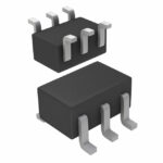 HN1C03FU-B,LF
The activity of extra discounts on wholesale prices is in full swing…
Please fill in your contact information and we will send you the latest wholesale price list.





